Rad-Hard Electronics and Trusted Services
Sandia’s Microsystems Center affords access to trusted resources and facilities for research and development, design, layout, fabrication, characterization, packaging, and test
Custom Solutions
Trusted Electronic Microsystems
The Sandia National Laboratories Microsystems Engineering and Sciences Applications (MESA) complex has achieved Defense MicroElectronics Activity (DMEA) Category 1A Trust Accreditation for trusted services including design, fabrication, packaging, and testing of electronic microsystems for both unclassified and classified integrated circuits.
Sandia’s Application-Specific Integrated Circuit (ASIC) team develops and maintains digital, analog, and mixed-signal design expertise, along with a deep understanding of technology offerings and design methodologies to provide custom microelectronic products and engineering services that fulfill diverse customer needs. Sandia focuses on developing unique, high reliability custom solutions for high consequence applications. Fabrication and Testing Capabilities.
Sandia is a leader in developing radiation hardened integrated circuit technologies and components for space and man-made environments. The Radiation Hard SOI CMOS7 technology is designed to survive strategic levels of radiation and the ASIC design process for either custom, ViArray, or mixed-signal based products is matched to meet these requirements. Subject matter experts are available to translate radiation environment specifications into radiation qualification protocols, and can develop a test plan that meets the customer’s requirements. Sandia can also partner with customers who are working with a rad-hard by design vendor to ensure that all radiation requirements can be met. As IC technologies scale below 90 nm feature size, total ionizing dose requirements are easier to meet, while transient rad effects, such as single-event effects and dose rate, are more challenging. Mitigating these effects require a broad range of capabilities and a wide knowledge of radiation effects. Sandia has well over a 100 year of experience among the technical staff to meet this challenge.
Custom radio frequency integrated circuits (RFICs) or monolithic microwave integrated circuits reduce size and weight without sacrificing performance. Sandia’s RF & Opto Microsystem department has demonstrated expertise in custom integrated circuit designs for radar and communication applications using advanced modeling and characterization techniques.
Sandia provides custom compound semiconductor microelectronics solutions. These include surface-normal and guided-wave optoelectronics, optical and microwave microelectromechanical devices and systems, compound semiconductor epitaxy, and rad-hard and high-power density microelectronics.
Silicon Foundry Access
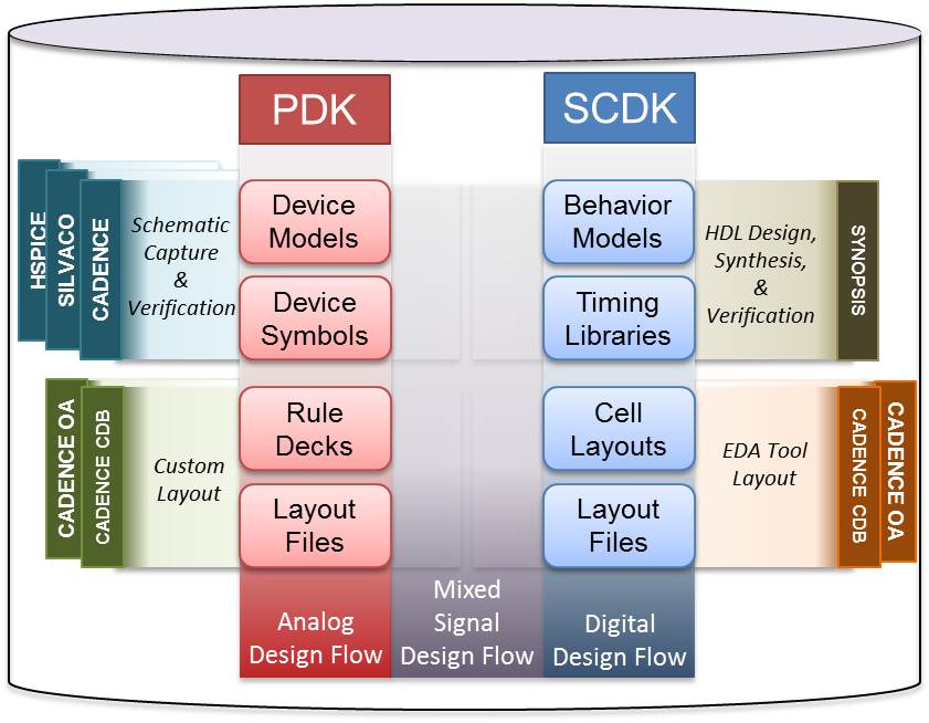
The focus of Sandia’s Silicon Fab is the development, application, and production of radiation-hardened complementary metal–oxide–semiconductor (CMOS) integrated circuit technologies capable of realizing digital, analog, mixed-mode, and nonvolatile memory circuits for the nuclear stockpile. In addition, Sandia’s silicon wafer fab is the world’s premier R&D source of surface micromachining technology. The facility includes 12,500 square feet of Class 1 clean room space. The silicon foundry is the primary supplier of custom rad-hard integrated circuits for weapon life extension programs and satellite systems. Foundry access is available via mechanisms such as the Multi-Project Wafer program and fast turn product capability is available through Structured ASIC technology. A process design kit (PDK) based on industry an standard CAD tool flow is available to facilitate external fab access.
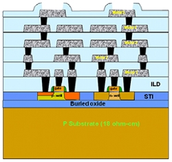
The CMOS7 technology is a 0.35 micron, 3.3 volts, shallow-trench-isolated (STI), partially-depleted, radiation-hardened, SOI (silicon on insulator) technology featuring five level metal, stacked contacts and vias, with salicided poly and source/drain regions. Key features include a low-vth PFET option and stackable metal-insulator-metal (MIM) capacitors. The five levels of W-plug/AlCu interconnect are planarized using chemical-mechanical polishing (CMP) techniques. High valued resistors are implemented for enhanced SEU (single-event-upset) protection. The Busfet structure is currently employed on all n-channel transistors to enhance both SEU and TID (total ionizing dose) response as well as to provide body ties. Full body ties are implemented in this technology on both n-channel and p-channel devices.
For more information see the CMOS7 Fact Sheet.
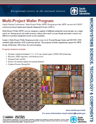
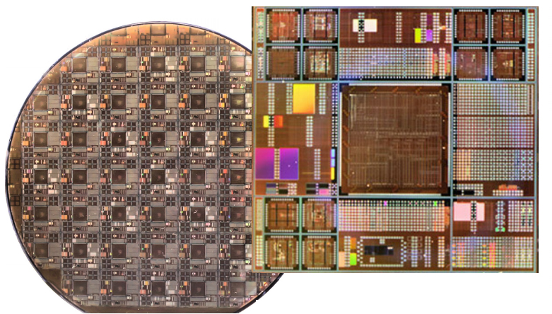
Sandia’s Multi-Project Wafer (MPW) Program provides MPW services for radiation-hardened Application-Specific Integrated Circuits (ASICs). MPW services combine a number of different integrated circuit designs on a single reticle set. Sharing mask and wafer resources reduces the overall cost per design and makes it more cost-effective to produce integrated circuits in low quantities.
Sandia National Laboratories’ Multi-Project Wafer Program offers access to its Trusted Design Center and ISO 9001:2000 certified, high-reliability ASIC production facility. The program includes engineering support for MPW design, technology, fabrication, test and packaging, all in a trusted environment.
The MPW Program has been available to external customers since 2010.
Program features include:
- Strategic radiation-hardened 3.3V, 0.35μm mixed-signal CMOS-Silicon On Insulator (SOI) technology
- Mixed signal design capability including precision resistors, MIM capacitors, and diode passives
- Standard Cells and IO
- Library of digital and analog intellectual property (IP) cells
- Cadence based Process Design Kit (PDK)
For more information, please see the Multi-Project Wafer Program Fact Sheet.
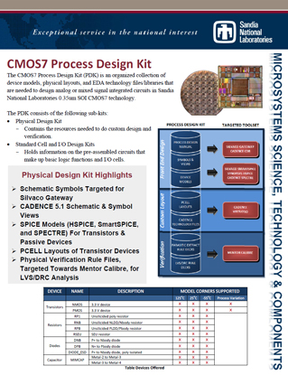
The CMOS7 Process Design Kit (PDK) is an organized collection of device models, physical layouts, and electronic design automation (EDA) technology files/libraries to support design of analog or mixed signal integrated circuits using Sandia’s 0.35um SOI CMOS7 technology.
For more information see the CMOS7 Process Design Kit (PDK) Fact Sheet.
Sandia National Laboratories’ Structured Application-Specific Integration Circuit (ASIC) provides a radiation-hardened, via-configurable implementation platform with ASIC-like performance. Structured ASICs enable rapid turn-around and lower Non-Recurring Engineering (NRE) and development costs. Pre-qualified base arrays reduce development risk, while open architecture minimizes Diminishing Manufacturing Sources (DMS) issues. The ViArray Structured ASIC enables safe, secure, user-defined trusted hardware, and the regular, fabric-like structure enhances verifiability of trusted parts.
For more information see the ViArray Fact Sheet.
R&D
The Research and Development website is currently under development.