Enabling Photonic/Electronic Microsystems
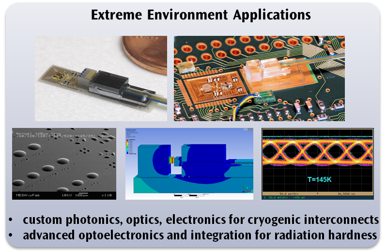
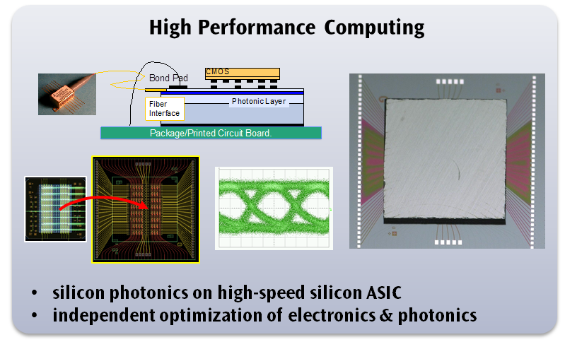
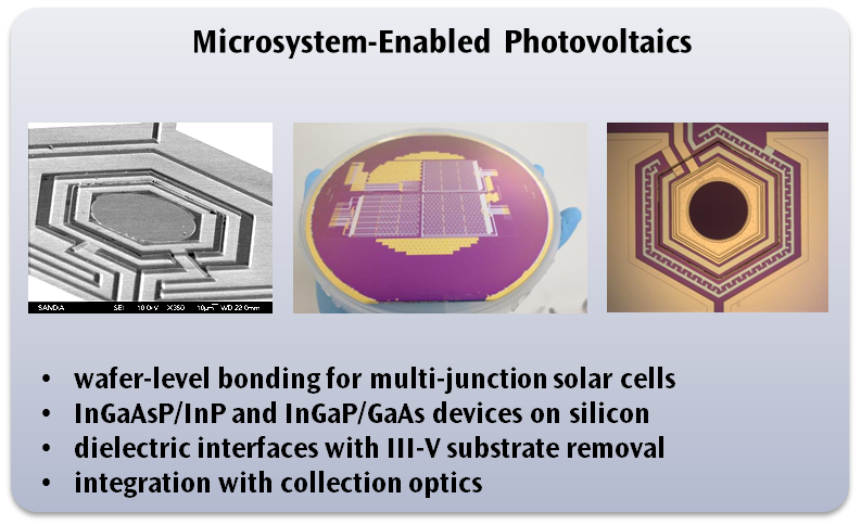
Sandia National Laboratories has developed several state-of-art hybridization capabilities to enable prototyping of high performance optoelectronic systems and microsensors for national security applications. Intimate integration of dissimilar materials allows the use of optimized photonic devices, optical elements, and electronic circuitry while improving overall system performance compared to conventional packaging approaches.
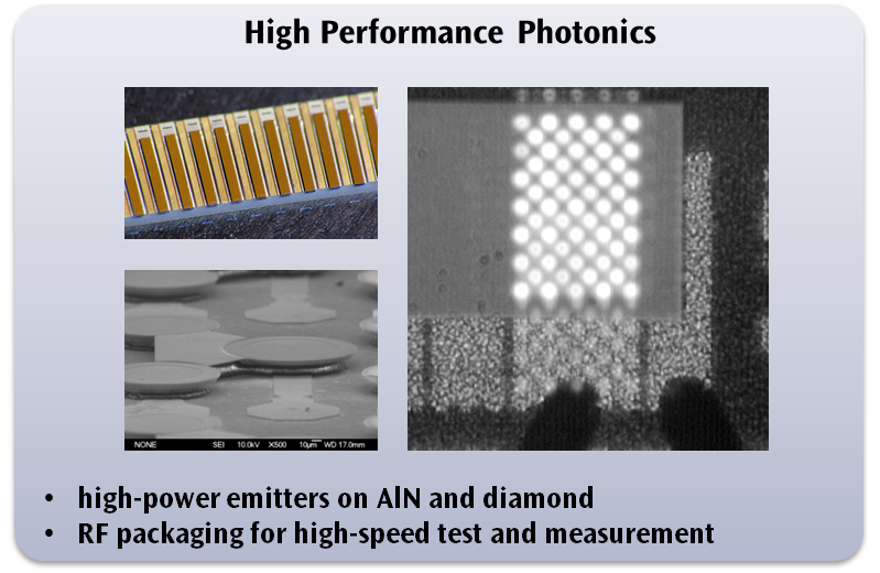
Heterogeneous integration processes leverage the Sandia MESA MicroFab facility, a 16,600sq-ft class-10 cleanroom with an extensive microfabrication tool set. Relevant integration methods range from wafer bonding of materials prior to microfabrication, to precision flip-chip attach of devices after processing is completed. Microsystems targeting a wide range of applications have been demonstrated, combining materials such as silicon, InP, GaAs, GaSb, AlN, diamond, and glass.