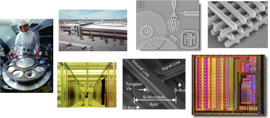
Leveraging the extensive CMOS production fabrication and testing capabilities in Sandia’s MESA facility (Figure 1), over the past 8 years, Sandia has engineered a mature silicon photonics process (see Figure 2). The silicon photonics process is an electro-optical silicon photonic integrated circuit platform built on silicon on insulator (SOI) wafer technology. The platform includes two waveguide interconnect layers (in silicon and silicon nitride), a full suite of dopant implants to provide active p-n junction formation and low ohmic contacts, and metal interconnect with optical cladding layers. Sandia’s silicon photonic process represents a mature process technology upon which to develop novel photonic integrated circuits and systems. This silicon photonics process has enabled numerous best in class device demonstrations, including record lowest energy optical modulators, record high speed Ge photodiodes, high speed optical modulators and resonant frequency locking of microring resonator filters and modulators.
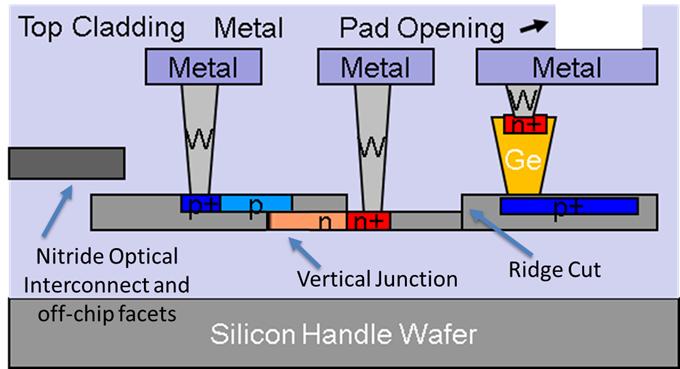
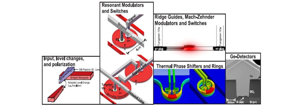
Figure 2 Overview of the silicon photonics process at the MESA fabrication facility
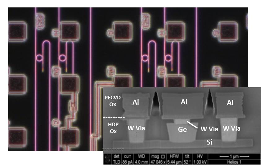
Figure 3 Ring resonator filters and Ge detector grown on Si waveguide cross section
Using the existing silicon photonics platform, Sandia has demonstrated many leading-edge silicon photonics devices for applications in communications, sensing, and computing. Among the highlights:
- The lowest energy resonant modulator at < 1 fJ/bit
- Full telecommunications C-band tunable resonant second-order filters
- Reconfigurable 2 x 2 wavelength selective switches and broadband switches with nano-second and sub-nanosecond switching times, integration of a micro-heater, sensor and modulator which were used to demonstrate thermal stabilization of resonant wavelength over 55C using scalable wavelength locking techniques
- Demonstration of an ultra-low V-pi*length product of < 1V-cm in a 10 Gb/s Mach Zehnder modulator and modulators with 3 dB bandwidths above 20 GHz
- Demonstration of an error free ‘long haul’ communications link using silicon photonics resonant modulators over 70 km
- Measurement and analysis of uniformity of manufactured resonant wavelength
- Ultra-sensitive room temperature infrared sensors with 1550 nm optical readout
- Low voltage compact broadband phase modulators and 2 x 2 thermo-optic switches
- Silicon photonics modulators with our strategic radiation-hardened 0.35 um CMOS, demonstrating a 2 Gb/s modulator driver and resonant modulator
- Record 45 GHz bandwidth Germanium detectors in Sandia’s silicon photonics process
Sandia has developed new processes for fabricating suspended active silicon photonic structures and is also making important contributions to the theory and demonstration of nanoscale optomechanical and phononic crystal devices, where the nanoscale light-matter within waveguides and other structures are opening new doors for ultra-high frequency transduction, sensing, and signal processing.
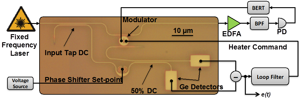
Figure 4 Balanced Homodyne Detector based Modulator Stabilization System
In 2014, Sandia successfully delivered hundreds of Si photonics dies to four universities that are part of the National Science Foundation’s Engineering Research Center for Integrated Access Networks (CIAN). In this first multi-project run with external collaborators, Sandia offered reticle space alongside its photonic designs. A Sandia Silicon Photonic Design Manual, as well as programming scripts for design and layout, were provided to the MPW users prior to the layout submission, enabling them to create custom photonics designs and take full advantage of existing device designs and smooth reticle integration. Sandia is open to partnering with other interested parties in developing a Si photonics design kit (PDK) that supports the IMI community. Sandia also invites discussions with commercial foundries interested in adopting the Sandia Silicon Photonics Process technology for high-volume production to support IMI.
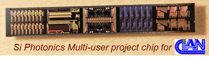
Figure 5 Si Photonics Multi-user project chip
Sandia has conducted many past and active R&D programs in the broad area of silicon-based photonics with scientific, national security, and commercial interests. The Sandia photonics team is currently leading a large internal R&D program in Quantum Communications with a goal to demonstrate a quantum key distribution (QKD) network with chip-scale transceiver nodes. The team recently completed a large project in exascale computing, to demonstrate low-energy silicon photonic transceivers with integration of state-of-the-art digital electronics. Other related efforts include Laboratory Directed Research & Development (LDRD) projects to integrate silicon photonics with focal plane arrays to enhance communication bandwidth and performance.
Sandia has supported many DOD efforts such as DARPA programs for Si Photonics for on-chip communications (UNIC), ultra-low power switching (ZOE), chip-scale optical phased arrays (SWEEPER), and optomechanical RF Photonics (MESO). This extensive national resource in Silicon photonics is available to collaborate with commercial and university partners in overcoming unique photonics challenges, productizing technologies from Sandia’s research efforts, and leveraging over 25 issued and pending patents.