State-of-Art Compound Semiconductor Photonics
Photonic Integrated Circuits and Lasers
Sandia National Laboratories has state-of-art photonic integrated circuit (PIC) design and fabrication capabilities and more than a decade of experience in the InP-based PIC technology. Sandia has proven and documented capabilities to monolithically integrate single-wavelength tunable diode lasers, modulators, amplifiers and interconnection optical waveguides on InP substrates for operation at telecom wavelengths. This capability rests on a foundation of state-of-the-art III-V semiconductor crystal growth and regrowth using metal-organic chemical vapor deposition (MOCVD) and post-growth quantum-well band-gap modification using quantum-well intermixing (QWI) methods to achieve the multiple band-edges and optical confinement needed for highly-functional PICs. PIC design and simulation is supported by experienced PhD-level staff spanning the complete design spectrum from optical guided-mode solvers and device electronics to complete optical circuits using eigenmode expansion, finite-difference time-domain, beam propagation methods.
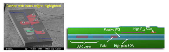
The images illustrate the sophisticated monolithic integration of passive waveguide photonics elements (such as waveguides, modulators, and switches) as well as active photonics elements including lasers, optical amplifiers, and photodetectors onto a single PIC. The capability enables compact high-performance PIC functions of integrated transmitter lasers and modulators, coherent optical receivers, and advanced telecom optical modulation formats such as DQPSK in single-chip platforms.
VCSELs
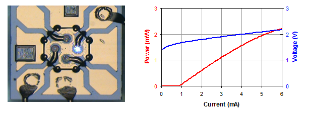
Vertical-Cavity Surface-Emitting Lasers Vertical-Cavity Surface-Emitting Lasers (VCSELs) achieve the lowest power consumption of any electrically driven lasers; with typical threshold currents between 0.5 and 1.0 mA and operating voltages less than 2 V they can run continuously on two AA batteries for several months. Other desirable attributes of VCSELs are high modulation bandwidth (10 GHz typical), circular output beam for coupling to optical fibers, high electron-to-photon differential quantum efficiency (50% typical), inherent single-longitudinal-frequency mode operation, and small cavity volume (a cylinder approximately 8 microns tall and 8 microns in diameter). These properties make VCSELs highly attractive for low-power optical microsystems that include: lasers, lenses and other optical elements, photodiodes, and standard integrated circuits for laser driving and photodiode sensing. The images below show a single-frequency 850-nm VCSEL driven at 2 mA and its properties (output optical power and voltage drop) versus drive current from 0 to 6 mA, exhibiting a threshold current of 0.9 mA.
Sandia has a unique ability to develop novel VCSEL devices using proprietary research capabilities developed over the past 20 years that are not commercially available. Sandia has been recognized as a leader in VCSEL research since the early 1990s, with over 1000 research publications and an extensive portfolio of intellectual property. The VCSEL research activity at Sandia is vertically integrated, with a unique breadth of in-house capabilities spanning VCSEL design, modeling, epitaxial semiconductor growth, cleanroom microfabrication, electrical characterization, optical characterization, and heterogeneous microsystem integration. Most recently, Sandia has developed single-frequency tunable VCSELs for atomic spectroscopy and MEMS interferometer sensors, spanning a range of custom wavelengths from 750 to 1050nm.
Focal Plane Arrays
Sandia National Laboratories has a long history and expertise in the development and demonstration of advanced infrared focal plane array (FPA) materials, devices, and data processing. Current R&D projects are centered on nBn FPAs in the shortwave, mid-wave, and long-wave infrared bands, leveraging novel III-V materials in phosphides and antimonides. Sandia has consistently demonstrated the highest material and device performance and is leading the development of cutting-edge infrared sensors, pushing the envelope of resolution and performance. Furthermore, advanced photonic integration concepts and methods are being developed to realize greater functionality of infrared sensors, such as agile spectral sensing and hyperspectral imaging, to enhance mission quality while driving down size, weight, power, and cost. Capabilities include multiple molecular-beam epitaxy reactors, large-format FPA fabrication/hybridization, and advanced nanoscale lithography.
Fabrication Facilities
Fabrication leverages the Sandia MESA MicroFab facility for III-V semiconductor electronics and photonics. This comprises a 16,600 sq ft class-10 cleanroom with capabilities spanning semiconductor crystal growth, complete processing with state-of-art direct-write electron-beam and projection stepper lithography with 2-6 inch wafer handling. The facility represents a Department of Energy investment in the creation, development, and prototyping of optoelectronics spanning TRL1-6+. Portions of the MESAFAB activity are compliant to NNSA QMS/QC-1/10 requirements, and a subset of this is Defense Microelectronics Activity (DMEA) certified as Trusted.
Examples
High Speed Digital Optical Systems
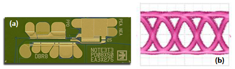
Recent Sandia programs in high-speed digital optical data COM communications are illustrated by the pair of images above showing an all-optical logic PIC performing a logical NOT function at 40 Gb/s. On this PIC an optical fiber data stream is input at the lower left corner. The data is optically amplified and then the inverse data (NOT output) transferred to an output optical beam sourced from the on-chip distributed Bragg reflection (DBR) laser and sent out of the PIC at the right edge. At right is a 40 Gb/s eye diagram taken from a high-speed waveguide photodiode exhibiting 40 mW input optical saturation power.
Radio Frequency Photonics
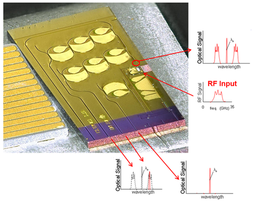
Another Sandia PIC development project is a highly functional PIC for the channelization of wideband radio frequency (RF) signals. The image above shows the PIC with illustrated input and output signals. This monolithic InP PIC integrates low-loss optical ring resonator filters with an on-chip wavelength tunable DBR laser to achieve parallel notch filtering (channelizing) in the optical domain of an input RF signal. Filters are 1-3 GHz wide. This optical domain RF filter function built into the PIC enables a dramatic reduction in size, weight and power compared to conventional electronics.
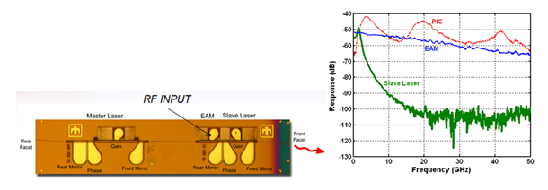
The final example, shown above, is the Sandia PIC using mutual injection locking of monolithically integrated coupled-cavity DBR lasers and modulators to exploit on-chip optical coupling to push the data modulation bandwidth of coupled lasers well beyond the fundamental limits of individual lasers. In this case, the coupled laser PIC is capable of modulation beyond 40 GHz where the individual lasers function only to ~3 GHz.