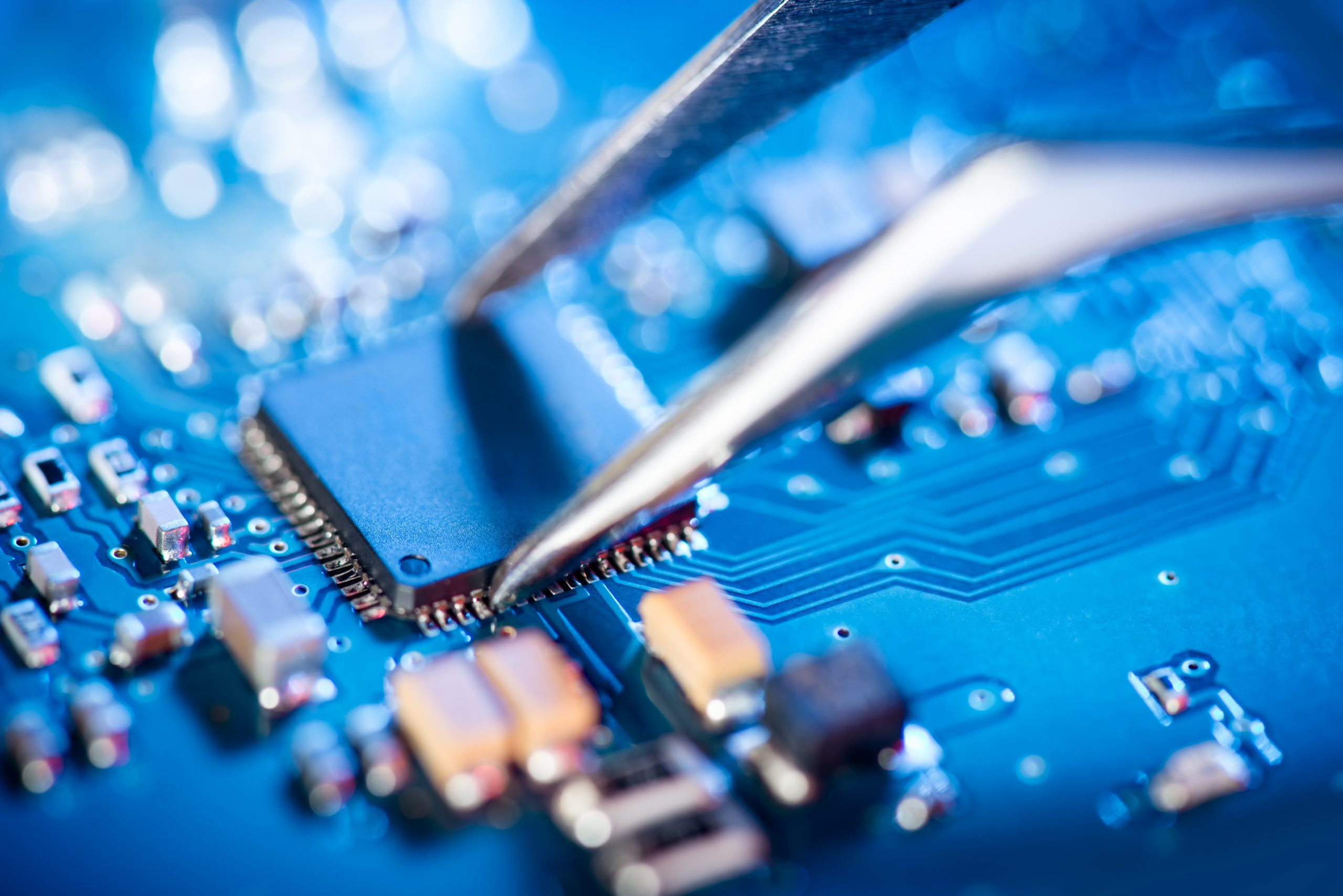
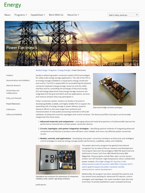
Power Electronics
Power electronics is the application of solid-state electronics for routing, control, and conversion of electrical power.
Custom Solutions
Wide-Bandgap
Wide-bandgap semiconductor materials such as silicon carbide (SiC) and gallium nitride (GaN) have the potential to revolutionize the field of power electronics. Sandia National Laboratories is well-suited to understand both performance and reliability in wide-bandgap power electronics.
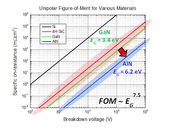
SiC and GaN have material properties that make them well suited for demanding power environments where switching devices are subjected to high voltage, current, and temperature. These properties, such as wide bandgaps, high breakdown voltage, and high thermal conductivity, suggest they could be used to fabricate devices that would be competitive with well-established Si technology. However, the long-term reliability of these materials must be studied before that becomes a reality.
Sandia National Laboratories is well-suited to understand both performance and reliability in wide-bandgap power electronics. Sandia’s Microsystems Engineering and Sciences Applications (MESA) facility houses experts in both Si and compound semiconductor growth and processing, as well as experts in material and device characterization and reliability. A well-established solid-state lighting program has studied the epitaxial growth of GaN by metal organic chemical vapor deposition (MOCVD) for nearly a decade, and associated electrical and optical characterization labs exist to ascertain the physics of the materials and devices. Additionally, Sandia possesses highly regarded reliability and failure analysis capabilities that have long supported Sandia’s complementary metal–oxide–semiconductor (CMOS) process. Sandia’s uniquely broad expertise, ranging from materials science up to grid-level power systems, ensures that fundamental understanding is utilized to improve power distribution for the benefit of the nation.
In order to deploy robust next-generation power conversion systems, it is necessary to understand the fundamental physical factors limiting semiconductor switch performance and reliability, since these switches are the heart of the power conversion system. In collaboration with industry and university partners, Sandia is studying the properties of both bulk and interface defects in SiC that could affect the properties of field-effect and bipolar devices based on this material. In field-effect devices such as power metal–oxide–semiconductor field-effect transistors (MOSFETs), bulk and interface defects associated with the gate oxide of the transistor may lead to shifts in its current-voltage characteristics, which can ultimately lead to reduced system efficiency or even catastrophic failure.
Sandia is also studying the properties of defects in GaN High-Electron Mobility Transistors (HEMTs). Combining expertise in areas including electrical device characterization, numerical modeling, optical spectroscopy, and atomic-force microscopy, the properties of surface and bulk defects in high-voltage HEMTs are being elucidated. Stress factors such as gate and drain voltage, which would be experienced by the HEMT in a working circuit, have been demonstrated to result in reduced performance and thus reduced system efficiency. The knowledge gained during performance and reliability characterization is used to improve the material growth and device fabrication processes.
Ultra Wide-Bandgap
The term “power electronics” is commonly used to refer to both the specialized power semiconductor devices and the circuits they comprise. Improving the Size, Weight, and Power (SWaP) of such devices, especially in harsh environments unique to Sandia’s mission space, has been identified as a critical strategic need.
Recent and rapid progress in wide-bandgap (WBG) power electronics (PE) based on SiC and GaN semiconductor materials has attracted significant attention and helped to spur Sandia’s interest. Despite these recent developments, the WBG PE industry is unable to create devices that fulfill Sandia’s unique mission requirements for performance and reliability in radiation environments. .
Sandia aims to leapfrog the current industry trajectory by developing a new generation of power electronics based on Ultra-WBG (UWBG) semiconductors (those with bandgaps greater than 3.4 eV), including high-Al-content aluminum gallium nitride (AlGaN), and by laying the foundation for predictive reliability and radiation hardness of these devices in environments required by Sandia mission areas.
Power Electronics Reliability
In order to facilitate the adoption of future energy technologies such as the smart grid, a fundamental shift in power electronics is needed to increase efficiency while simultaneously decreasing system size, power, and weight. Additionally, to reduce systems costs over the 20+ year lifetime applications require, these power electronics devices must be highly reliable. Sandia focuses on performance and reliability of power electronics components through the study of novel wide and ultra wide bandgap technologies, as well as energy conversion systems such as photovoltaic inverter systems.
The continued exponential growth of photovoltaic (PV) technologies paves a path to a solar-powered world, but requires continued progress toward low-cost, high-reliability, and high-performance PV systems. High reliability is an essential element in achieving low-cost solar electricity by reducing operation and maintenance (O&M) costs and by extending system lifetime and availability. However, these attributes are difficult to verify at the time of installation. Utilities, financiers, homeowners, and planners are demanding this information in order to evaluate their financial risk as a prerequisite to large investments. Reliability research and development (R&D) is needed to build market confidence by improving product reliability, predictions of system availability, O&M cost, and system lifetime.
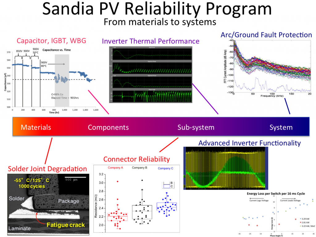
The Sandia PV Reliability Program is focused on understanding, predicting, and improving the reliability of PV systems through the study of the entire PV environment continuum, from materials to systems, using a “total systems” approach to address PV reliability, availability, maintainability, safety, and O&M. This approach considers the interconnectedness of all system components along with the design, implementation and feedback necessary to improve the operation of future PV systems. Sandia focuses on understanding gaps in current PV schemes, such as quantifying technical risks, selecting optimal designs schemes, and shaping real processes to moderate adverse outcomes.
The FY14-16 reliability program focuses on two primary research areas that encompass widespread reliability and safety issues in today’s PV systems: (1) PV arc-fault and ground fault issues; and (2) inverter reliability.
Arc/Ground Fault Reliability
Arc fault R&D efforts assist with the development of arc-fault detector/circuit interrupter certification standards through Underwriters’ Laboratory task groups and International Electrotechnical Commission Technical Committee 82 (IEC TC 82). Novel fault locating/prediction tools are being developed and analyzed to assist plant owners with troubleshooting PV systems after arc and ground fault detectors have tripped. Arc-faults in connectors and solder joints are being studied to find prognostic methods of preventing the arc. New ground fault technologies (isolation monitoring, residual-current detectors, current sense relays) are also be compared to traditional fuse-based solution, and new thresholds are being recommended for high-sensitivity detection without an increase in unwanted tripping events.
Inverter Reliability
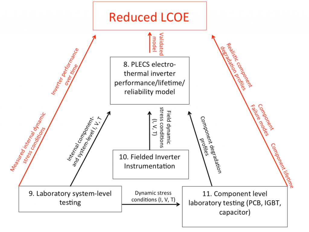
The Sandia research program focuses on the development, demonstration, and utilization of a comprehensive inverter system electro-thermal model (using Matlab/Simulink, COMSOL, PSPICE, and PLECS), with submodels that are accurate and fast, allowing for more robust design and optimization of inverter power electronics, thermal management and materials. This will reduce industry costs and facilitate the development of more reliable residential and utility-scale inverters with lifetimes of 25 years.
A robust and flexible model must be informed and validated by both field and experimental data. Successful predictive ability of the simulation is predicated on obtaining accurate information regarding system- and component-level electrical and thermal environments, as well as external usage environments. System-level instrumentation and testing is being carried out to determine the electro-thermal environments of components during inverter operation, both under “normal” usage conditions and advanced operating modes (e.g. non-unity power factor, high DC/AC ratios, voltage ride-through scenarios). These real, dynamic stress conditions are used to carry out component-level stress testing to determine accurate component degradation profiles, lifetimes, and failure mechanisms for use in inverter simulation. The simulations also utilize information regarding component- and system-level electro-thermal environments obtained from instrumented fielded inverters.
In order to make photovoltaics (PV) cost-competitive with traditional energy sources, the economies of scale have guided inverter design in two directions: large, centralized, utility-scale (~500 kW) inverters vs. small, modular, module-level (~200 W) power electronics (MLPE). MLPEs, such as microinverters and DC power optimizers, offer advantages in safety, system operations and maintenance (O&M), energy yield, and component lifetime due to their smaller size, lower power handling requirements, and module-level power point tracking and monitoring capability.
However, MLPEs suffer from two main disadvantages: first, depending on array topology (especially the proximity to the PV module), they can be subjected to more extreme environments (e.g. temperature cycling) during the day, resulting in a negative impact to reliability; second, since solar installations can have tens of thousands to millions of modules (and as many MLPE units), it may be difficult to track and repair units as they go out of service. Therefore, the statistical reliability of each device and the extension of unit lifetime are of critical importance to the O&M schemes of large solar installations.
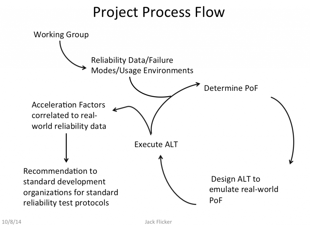
While an overwhelming majority of time and research has focused on PV module efficiency and reliability, these issues have been largely ignored for the balance of system components. As a relatively nascent industry, the PV power electronics industry does not have the extensive, standardized reliability measuring accelerated lifetime tests (ALTs) that exist in the module industry or other more mature power electronics industries (e.g. automotive). Sandia’s PREDICTs program is focused on recommending standard ALTs that have been thoroughly correlated to fielded MLPE failure rates, modes, and environmental stressors. Through ALTs the confidence of system operators, integrators, manufacturers, and financiers is increased, decreasing the cost of financing and operating large solar installations.
In order to accomplish this goal, Sandia National Laboratories is leading a team of research institutions that will carry out work in five different task areas over the 3 year time period of this project. These tasks include:
- Formation of a MLPE reliability working group to gather MLPE usage statistics, device/system information, operating environments, and reliability data
- Analysis of physics of failure (PoF) for products in the field and accelerated test plan development to exacerbate those failure mechanisms
- Accelerated testing, acceleration factor determination, and correlation to field reliability
- Submission of recommended reliability standard protocol to standards development organizations
R&D
For more information about Research and Development in this area please visit Nanodevices and Microsystems.
Fact Sheets, Publications, References, Animations, Licensing IP Opportunities
Energy Storage – Power Electronics
Energy PV Performance and Modeling
Power Electronics Publications
GaN:
R. J. Kaplar, J. Dickerson, S. DasGupta, S. Atcitty, M. J. Marinella, S. G. Khalil, D. Zehnder, and A. Garrido, “Impact of Gate Stack on the Stability of Normally-Off AlGaN/GaN Power Switching HEMTs,” presented at International Symposium on Power Semiconductor Devices (June 2014).
S. G. Khalil, L. Ray, M. Chen, R. Chu, D. Zehnder, A. Garrido, M. Munsi, B. Hughes, K. Boutros, R. J. Kaplar, J. Dickerson, S. DasGupta, S. Atcitty, and M. J. Marinella, “Trap-Related Parametric Shifts under DC Bias and Switched Operation Life Stress in Power AlGaN/GaN HEMTs,” presented at International Reliability Physics Symposium (June 2014).
S. DasGupta, A. Armstrong, R. Kaplar, M. Marinella, J. Stanley, M. Smith, S. Atcitty, M. Sun, and T. Palacios, “Impact of the Al Mole Fraction on the Bulk- and Surface-State-Induced Instability of AlGaN/GaN HEMTs,” Materials Research Society Spring Meeting, San Francisco, CA (April 2012).
S. DasGupta, M. Sun, A. Armstrong, R. Kaplar, M. Marinella, J. Stanley, S. Atcitty, and T. Palacios, “Slow Detrapping Transients due to Gate and Drain Bias in High Breakdown Voltage AlGaN/GaN HEMTs,” IEEE Transactions on Electron Devices 59 (8), 2115 (2012).
R. Kaplar, M. Marinella, S. DasGupta, M. Smith, S. Atcitty, M. Sun, and T. Palacios, “Characterization and Reliability of SiC- and GaN-Based Power Transistors for Renewable Energy Applications,” IEEE Energy Tech (May 2012).
S. Atcitty, R. Kaplar, S. DasGupta, M. Marinella, M. Smith, M. Sun, and T. Palacios, “Wide-Bandgap Power Switch Reliability for Energy Storage and Grid Applications,” Advanced Microgrid Concepts and Technologies Workshop, Beltsville, MD (June 2012).
R. Kaplar, S. DasGupta, M. Sun, M. Marinella, S. Atcitty, and T. Palacios, “Reliability Characterization of High Voltage HEMTs under the GIGA Program,” GIGA Program Review at MIT (August 2012).
R. Kaplar, S. DasGupta, M. Sun, M. Marinella, L. Biedermann, A. Armstrong, S. Atcitty, T. Palacios, and J. Simmons, “Characterization and Modeling of Charge Trapping and Recovery in High-Voltage AlGaN/GaN HEMTs,” Hughes Research Laboratories seminar, Malibu, CA (October 2012).
(Invited) S. Atcitty, R. Kaplar, S. DasGupta, M. Marinella, A. Armstrong, L. Biedermann, M. Sun, T. Palacios, and M. Smith, “GaN-Based Wide-Bandgap Power Switching Devices: From Atoms to the Grid,” ECS Transactions 50 (3), 199 (2012).
R. Kaplar, “Materials Issues for Wide-Bandgap Power Electronics Devices,” Oak Ridge National Laboratory Wide-Bandgap Devices for Vehicle Applications Workshop (November 2012).
S. DasGupta, L. B. Biedermann, M. Sun, R. J. Kaplar, M. J. Marinella, K. R. Zavadil, S. Atcitty, and T. Palacios, “Role of Barrier Structure in Current Collapse of AlGaN/GaN High Electron Mobility Transistors,” Applied Physics Letters 101, 243506 (2012).
R. Kaplar, S. DasGputa, M. Sun, M. Marinella, L. Biedermann, A. Armstrong, D. Hughart, S. Atcitty, and T. Palacios, “Characterization and Reliability of SiC- and GaN-Based Power Transistors,” United Technologies Research Center seminar, Hartford, CT (February 2013).
R. Kaplar, M. Marinella, S. DasGupta, D. Hughart, L. Biedermann, S. Atcitty, and J. Simmons, “Wide-Bandgap Power Semiconductor Research at Sandia National Laboratories,” Auburn University Physics Department colloquium, Auburn, AL (March 2013).
S. DasGupta, L. Biedermann, M. Sun, R. K. Kaplar, M. J. Marinella, K. Zavadil, S. Atcitty, and T. Palacios, “Influence of Barrier Design on Current Collapse in High Voltage AlGaN/GaN HEMTs,” IEEE International Reliability Physics Symposium, Monterey, CA (April 2013).
R. Kaplar, “Wide-Bandgap Semiconductors for Power Electronics,” KLA-Tencor seminar (April 2013).
R. Kaplar, S. DasGupta, M. Sun, M. Marinella, S. Atcitty, and T. Palacios, “Recent Work on Reliability Characterization of High Voltage HEMTs under the GIGA Program: Interaction of Deep Levels with Quantum Well States,” GIGA Program Review at IQE (May 2013).
M. J. Marinella, S. DasGupta, R. J. Kaplar, M. Sun, S. Atcitty, and T. Palacios, “Effect of Interaction of Deep Level Defects with Quantum Well States on Detrapping Transients in High-Voltage AlGaN/GaN HEMTs,” presented at 224th Meeting of the Electrochemical Society (October 2013).
SiC:
R. Kaplar, D. Hughart, S. Atcitty, J. Flicker, S. DasGupta and M. Marinella. “Performance and Reliability Characterization of 1200 V Silicon Carbide Power MOSFETs at High Temperatures,” Proceedings of the International Conference and Exhibition on High Temperature Electronics Network (HiTEN), 2013.
M. Marinella, D. Hughart, J. Flicker, S. DasGupta, S. Attcity and R. Kaplar. “Progress in SiC MOSFET Reliability,” ECS Transactions, Vol. 58 (4), pp 211-220, 2013.
D. R. Hughart, J. D. Flicker, S. Attcity, M. J. Marinell, and R. Kaplar. “Sensitivity Analysis of a New Technique for Trapped Charge Extraction in SiC MOSFETs from Subthreshold Characteristics,” Proceedings of International Reliability Physics Symposium, pp 2C.2.1-2C.2.6, 2014.
J. Flicker, D.Hughart, R. Kaplar, S. Atcitty and M. Marinella. “Characterization of Reliability in SiC Power Devices,” The Electrochemical Society Transactions, In Press 2014.
J. Flicker, D. Hughart, R. Kaplar, S. Atcitty and M. Marinella. “Performance and Reliability Characterization of 1200 V Silicon Carbide Power MOSFETs and JFETs at High Temperatures,” High Temperature Electronics Conference, 2014.
Arc/Ground Fault:
J. D. Flicker and J. Johnson. “Analysis of Fuses for ‘Blind Spot’ Ground Fault Detection in Photovoltaic Power Systems,” Solar American Board for Codes and Standards Technical Report, June 2013.
G. Ball, B. Brooks, J. Johnson, J. Flicker, A Rosenthal, J. Wiles, L. Sherwood, M. Albers and T. Zgonena. “Inverter Ground-Fault Detection ‘Blind Spot’ and Mitigation Methods,” Solar American Board for Codes and Standards Technical Report, July 2013.
M. Alam, F. Khan, J. Johnson, and J. Flicker. “PV Ground-Fault Detection Using Spread Spectrum Time Domain Reflectometry (SSTDR)” Proceedings IEEE Energy Conversion Congress and Exposition (ECCE), pp 1015-1020, 2013.
J. D. Flicker and J. Johnson. “Electrical Simulations of Series and Parallel PV Arc-Faults” Proceedings Photovoltaics Specialists Conference (PVSC), pp 3165-3172, 2013.
M. Alam, F. Khan, J. Johnson and J. Flicker. “PV Faults: Overview, Modeling, Prevention and Detection Techniques” Proceedings IEEE Workshop on Control and Modeling for Power Electronics (COMPEL) 2013.
M. Alam, F. Khan, J. Johnson and J. Flicker, “A Comprehensive Review of Catastrophic Faults in PV Arrays: Types, Detection and Mitigation Techniques.” Progress in Photovoltaics, Accepted 2014.
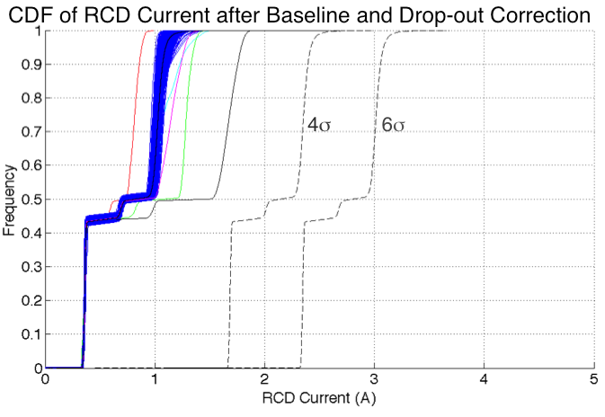
J. Flicker, J, Johnson, M. Albers and G. Ball. “Recommendations for RCD and Riso Ground Fault Detector Trip Thresholds” Photovoltaics Specialists Conference (PVSC), 2014.
J. Flicker, K. Armijo and J. Johnson. “Recommendations for RCD Ground Fault Detector Trip Thresholds” European Photovoltaics Specialists Conference (EUPVSEC), 2014.
Inverter Reliability:
J. D. Flicker, R. Kaplar, B. Yang, M. Marinella, and J. Granata. “Insulated Gate Bipolar Transistor Reliability Testing Protocol for PV Inverter Applications.” Progress in Photovoltaics. Vol. 22 (9), pp 970-983, 2012.
J. D. Flicker, R. Kaplar, M. Marinella, and J. Granata. “PV Inverter Performance and Reliability: What is the Role of the Bus Capacitor?” Proceedings Photovoltaics Specialists Conference (PVSC), 2012.
J. D. Flicker, R. Kaplar, and J. Granata. “Lifetime Testing of Metallized Thin Film Capacitors for Inverter Applications” Proceedings Photovoltaics Specialists Conference (PVSC), pp 3340-3342, 2013.