Photonics Applications
Sandia’s mission in national security has fostered capabilities and technologies including Photonics, Photovoltaics, Focal Plane Arrays, Advanced Sensors, Optical MEMS, Plasmonics, and Metamaterials.
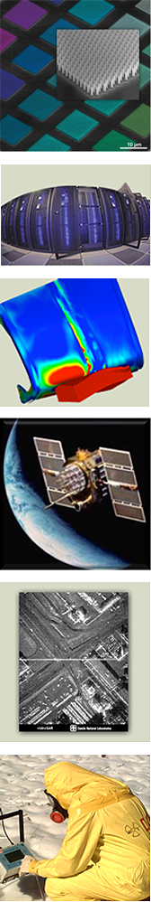
These capabilities in photonics support a board range of applications, from remote sensing in space and novel military RF communications to commercial photovoltaics and solid state lighting. Sandia’s research efforts will continue to accelerate innovation in technologies that benefit not only U.S. warfighters, but also the commercial sector. Under the IMI program, Sandia will partner with interested industry and university partners to further advance and maturate photonics technologies that strengthen U.S. security and economic well-being.
- Optical Interconnect for networking, computing, and sensor systems
- Optical Data Links for naval, ground, or space communication
- Infrared Detection for warfighters, homeland security, automotive and aeronautic applications
- Alternative Energy Sources to enable mobility and a clean, sustainable environment
- RF Signal Generation and Detection for radar and wireless communication
- Proximal and Standoff Detection for chemical and biological agents
- High-efficiency and cost-effective lighting
Fabrication Capabilities
CMOS Fab
The Silicon Fab has processing expertise in both CMOS and MEMS technologies. Over 150 equipment sets are maintained, supported and operated 24 hours per day, 5 days a week (3 shifts). Both processing and maintenance expertise are staffed on all 3 shifts. Sandia offers unique prototyping capabilities and is capable of producing full flow production lots with quick turnaround time, as well as performing flexible process development.
- High NA 248nm Deep UV Lithography with resolution down to 110nm and Ebeam lithography with 5nm resolution
- Security-based Application-Specific Integrated Circuits (ASICs)
- Trusted Design of Secure Microprocessors
- High-consequence, High-reliability ICs: ICs that cannot fail in extreme environments
- Low-noise Analog Electronics Designs: Low-power and asynchronous designs
- Sensor Readout Electronics (e.g. – Read-out Integrated Circuits for focal plane arrays)
- High voltage and novel MEMS interface electronics
- Special Processor/Accelerator Architecture and Designs
- Fast-turn, Radiation-Hardened Structured ASIC
- Novel Electronic System Modeling, especially for extreme environment reliability
- Prototype Memristor high-density low-power memory and switch matrices
- Prototype Graphene-based transistors, optoelectronics, and thermal interface materials
- Silicon, Optical, and Nano Technology Heteogeneous Integration
III-V Fab
Sandia’s III-V Fab offers wide variety of specialty compound semiconductor device technologies:
- Integrated (vertical-cavity surface-emitting lasers, resonant-cavity photodiodes circuits vertical-cavity surface-emitting lasers, resonant-cavity photodiodes (VCSEL-RCPD)
- Photonic integrated circuits (GaAs, InP)
- Planar lightwave circuits (SiON materials set) such as various optical guided-wave filters and switches
- Optical data links
- Micromirror arrays and subsystems for switch matrices and adaptive optics
- Radio-frequency switches and networks that include phase shifters and tunable filters
- Power amplifiers
- Low-noise amplifiers
- Rad-hard heterojunction bipolar transistors
- High-electron mobility transistors
- Wide-bandgap and ultrawide-bandgap power electronics devices
- Compound semiconductor nanowires, quantum dots, and other nanostructures
MEMS
Sandia fabricates microelectromechanical systems (MEMS) in both the Silicon Fab and the Compound Semiconductor Fab. The capabilities applied to MEMS include:
- Sub-micron photolithography and electron beam lithography
- Wet etch and deep reactive ion etch (DRIE)
- Polysilicon deposition and multilevel, polysilicon surface micromachining
- Deposition and etching of various metals, including aluminum and tungsten
- Deposition and etching of various oxides
- Deposition and etching of various nitrides, including aluminum nitride
We apply these capabilities to make research prototype devices, such as, micro-actuators, inertial and other sensors, and RF filters and oscillators. Sandia’s fabrication facilities enable us to integrate MEMS with photonics and other technologies through heterogeneous integration, chip stacking, and wafer-level packaging.