
Fundamental Science
Electrochemical research and development (R&D) and engineering serves as a theoretical and practical basis for the Metal Micromachining team. The study of electrochemical phenomena and use of analytical techniques provides a powerful set of tools to analyze and formulate precise and optimized plating conditions. This is required to realize unique combinations of metallic alloys with tailored crystallographic orientations and made-to-order grain sizes.
Success Stories
Pt electrodeposition for high temperature applications
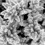
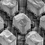
High surface area nickel electroformed nano structures for chemical sensor applications
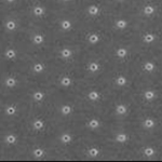
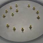
Electrochemical cell for analyte analysis constructed of nanoelectrode arrays (small dots) on segregated counted electrode (background)
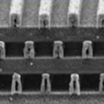
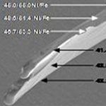
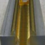
Cross-section of optimized composition magnetic Ni/Fe elecrtroforms
Surface contour plot of temperature vs. agiation operating parameters from a DOE study to optimize magnetic properties of Ni/Fe and Ni/Fe/Cr deposit films

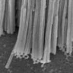
Cross-section of Bi2(Te, Se)^3 nano wires electrochemically synthesized in anodized aluminum oxide membrane for thermo-electrics study
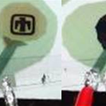
Electrochromic window in the on mode with image in background and EC window in the off mode blocking background image
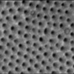
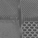
Electrochemically grown porous oxide with hexagonal ordered pores
Process Development
The Metal Micromachining Program maintains three fabrication labs dedicated to process development. Through large adjoining electroplating and lithography laboratories, a class 100 clean room, and a complete planarization laboratory with an e-beam evaporator, the team is capable of performing full-spectrum fabrication, as well as partial steps on an as-needed basis. Also, access to comprehensive fabrication laboratories and equipment allow proof of concept experiments to be performed (as a controlled environment is required to develop and maintain customized processes).
The ability to deviate from traditional methods and develop new processes allows the team to continually push the limits of what can be achieved.
Success Stories
Galvanic periodic reverse pulse compatible with Si-based ROICs designed to level and flatten the deposition
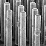
Current mission requirements continually push for a reduction in pixel size and pitch in focal plane arrays. To this end, electroforming indium bumps can greatly reduce pitch to lower levels than what lift-off patterning can traditionally achieve. However, early indium plating results yielded very poor uniformity. To solve this problem, the Metal Micromachining team developed a galvanic periodic reverse pulse compatible with Si-based ROICs designed to level and flatten the deposition. Since then, the electroplated indium has been hybridized, electrically tested and pull tested demonstrating plated indium as a viable alternative to evaporated indium.
Adding High Z Material using Si as Pre-Form
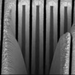
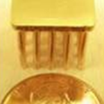
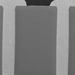
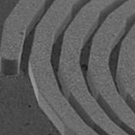
For the purposes of creating gratings for phase contrast imaging, Si alone is insufficient as an x-ray absorber. To mitigate this issue, a high Z material needed to be added using Si as a pre-form. The Metal Micromachining team employed two separate approaches to accomplish this. In both approaches—CVD tungsten and electroplated gold—the goal was to add 1 micron of high Z metal to each side of the Si post to create a 50 percent duty cycle metal grating. The SEM images of the FIB cross sectioned gratings show the CVD W only reached .5 micron thickness at the top of the grating and tapered to less than a quarter of micron within 3 microns of the top. In addition, the W stress was so great that a Parylene support coating was needed to keep the gratings from collapsing. In comparison, the gold electroplating process was tailored to conform to the Si and reached the 1 micron target thickness along the entire 26 micron height of the Si. The enabling technology was Robert Grubb’s atomic layer deposition of Pt that conformally metalized the Si gratings for subsequent electroplating. Using ALD for seed metal, the team plated a one micron gold coating on 50 micron tall Si gratings. This process is currently being scaled to 6†wafers.
Electrical conductivity
Deposited Gold coating on alloy 52 pins for electrical conductivity needs of NW components.
Diffusion bonding
Deposited Gold coating on copper heat sinks for battery application.
Metallic reflection for plasitcs
Polymer cavity device requiring coating of electroplated Gold coated inside liner.
Wear & fatigue resistance
Deposited Gold coating on NW component to meet mechanical and conductivity requirements.
Build up worn or undersized parts
Deposited Electroless Nickel coating on NW component to meet mechanical and corrosion requirements.
Magnetic insulation
Deposited Copper Stainless Steel mechanical device meet NW requirements.
Solderability
Deposited Gold coating on end caps to meet NW mechanical and conductivity requirements.
Reduced coefficient of friction
Deposited Gold coating NW component to meet mechanical and conductivity requirements.
Heat dissipation
Deposited Gold coating on copper heat sinks for battery application.
Metalization of plastic
Polymer based explosive shape charges lined with electrochemically deposited Copper and Gold liners to increase penetration depth for Military applications.
Product Realization
Electrochemical research and development (R&D) and engineering serves as a theoretical and practical basis for the Metal Micromachining team. The study of electrochemical phenomena and use of analytical techniques provides a powerful set of tools to analyze and formulate precise and optimized plating conditions. This is required to realize unique combinations of metallic alloys with tailored crystallographic orientations and made-to-order grain sizes.
Success Stories
Gold structure for controlling spatial beam patterns
Terahertz radiation becomes problematic when a need arises to move it from one place to another. However, the Metal Micromachining team solved this problem by fabricating solid metal waveguides. Rather than creating the device with a single mold with traditional approaches, the team developed methods to stack multiple layers using photolithography and electroplating to create 70-micrometer-tall, hollow, rectangular, gold waveguides. These innovative waveguides were fabricated directly onto non-planar semiconductor chips and coupled with terahertz lasers to make some of the first-ever terahertz integrated circuits.
Copper interconnects in Si through substrate vias
Collaborating with Lawrence Livermore National Laboratory and others, the team helped create a bio-electronic retinal implant capable of helping those suffering from retinal degenerative diseases. The Metal Micromachining team was responsible for fabricating the interface between the retina and the electronics – the precise task of electrofilling solid metal plugs into the holds across large arrays of through hole vias drilled out of various substrates. Designing a specialized fixture to provide electrical connection to the base of each via, the process has been successfully demonstrated with Cu in laster-drilled alumina, Pt in laser-drilled sapphire, Cu in photo-defined glass and most recently Cu in Si.
Gold concentric rings for high-voltage pulses
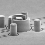
Electroformed Gold coil type structure for MEMS sensing device. Back side contact was possible by using tungsten fired electrically conductive through substrate vias using an alumina substrate.
Ni/Fe lattice for shifting photonic band gaps
Photonic crystal lattice electroformed in Gold, 1 mm diameter and 18 mm tall. Electrormed into x-ray exposed PMMA mold to create optimum vertical sidewall profile.
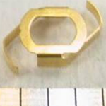
Gold structure for manipulating a single trapped ion
Two layer lithography process to Electroform a Gold Ion Trap in collaboration with NIST, Boulder site.