Microsystems and Engineering Sciences Applications (MESA)
The multi-mission environment of the Labs promotes a diverse, multi-disciplinary team of subject matter experts in fabrication labs and clean room facilities. Two important Sandia support labs – the Silicon Photonic Foundry and the III-V Photonic Integrated Circuit (PIC) Lab – are co-located inside the MESA facility under the same 65,000 square foot roof.
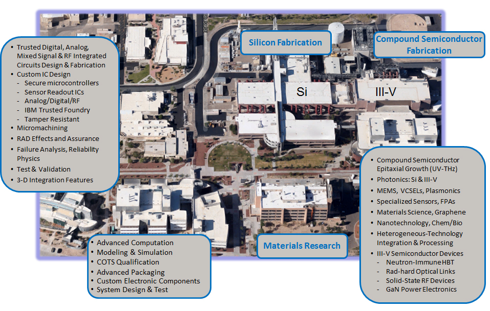
Sandia National Laboratories, located on Kirtland Air Force Base in Albuquerque, NM, executes a multi-mission national security role that supports a diverse multi-disciplinary team of subject matter experts in fabrication labs and clean room facilities. The Sandia Microsystems and Engineering Sciences Applications (MESA) facility is the only semiconductor fabricator within the United States that has a silicon (Si) complementary metal–oxide–semiconductor (CMOS), Si photonics and production III-V processing capability co-located in the same facility. This capability seamlessly mixes strategically rad-hard CMOS and III-V compound semiconductor product deliveries with leading edge R&D in microelectronics, photonics, MEMS, and quantum within a high-rigor and high-flexibility fabrication process flow. A fully Trusted accreditation status, as well as limited access control processing, are also valuable MESA facility attributes.
Sandia’s national security mission responsibilities for the National Nuclear Security Administration (NNSA) and other Department of Defense (DoD) agencies have developed deep expertise in photonics, photovoltaics, focal plane arrays, advanced sensors, optical MEMS, plasmonics/metamaterials, advanced packaging, and reliability/security (especially for extreme or high-consequence environments). Work in these areas spans theoretical analysis, device fabrication and test, and advanced pathfinder products.
As a government-owned resource for the National Security Photonics Center (NSPC), Sandia can support commercial foundry activities by providing additional capacity for design, fabrication, and systems integration from technology readiness level (TRL) 1 to TRL6, and with certification as a trusted foundry MESA can produce electronics intended for high-consequence military applications. For example, IMI customers might utilize the Silicon Photonics Foundry multi project wafer (MPW) system and III-V PIC foundry to access materials or devices outside the immediate scope of the IMI foundry to fabricate novel prototypes for evaluation in defense applications.
Several of Sandia’s current photonics projects utilize heterogeneous integration of III-Vs and Si photonics with CMOS to realize novel advanced pathfinder products for satellite sensing, exascale computing, next generation alternative energy, and specific radiation hardened and classified applications. Extensive testing and evaluation labs available at Sandia may also enable rapid impact of the IMI on new products by supporting university and industry partners in the development of the complete design, simulation, and test infrastructure needed for rapid, low-cost manufacturing. Sandia National Laboratories also routinely supports defense contractor partners in technology maturation and transfer activities, and university partners via R&D collaborations and student fellowships/internships within the Laboratories.
Fab Facility
The MESA facility comprises 400,000 sq ft of clean rooms and laboratories with providing a flexible fab with production rigor, adjacent Si and III-V cleanrooms, and all the standard fab & test tools. Over 150 equipment sets are maintained, supported and operated 24 hours per day, 5 days a week (3 shifts) in a secure environment with highly cleared staff. Tooling examples include: High NA 248nm Deep UV Lithography with resolution down to 110nm, E-beam lithography with 5nm resolution, NanoSEM CD metrology systems with LER capability for waveguide optimization, HDP oxide for cladding and low loss SiN for 2nd layer waveguides, Ion Implant, CMP and Deep Si Etch, 6 MOCVD and 4 MBE reactors for III-V growth, 3 FC-150 die level bonders, Silver and Gold electroplating, lift-off, wafer to wafer bonding and thinning.
III-V & Si Electronics
AlxGa1-xAs/GaAs, InxGa1-xAsyP1-y/InP, InxGa1-xAs /GaAs, AlGaN/GaN, InGaN, Si, SOI, AlN, Graphene. Full ASIC design using Cadence and Simulation via TCAD Silvaco, Sensor read out electronics (ROICs), Rad-Hard ASICs, structured ASICs, Secure Microprocessors, Low noise analog electronics design, III-V Amplifiers, Rad Hard Heterojunction Bipolar Transistors (HBT), High electron mobility transistors, Schottky Barrier Diodes, etc.
III-V & Si Photonics
Waveguides/devices in silicon, oxide, oxy-nitride, nitride, a-Si, a-Ge, InP, AlGaAs, InGaAs, GaN, Graphene. L-edit design and Lumerical, Silvaco simulation. VCSELs, DBR lasers, EAMs, High-gain & High-Psat SOAs, LEDs, Photonic Integrated Circuits (PICs) incorporating lasers, detectors, modulators, filters, Photovoltaics spanning UV to IR, Si photonic fj/bit modulators, integrated germanium detectors, low loss ridge and rib waveguides, 2 x 2 broadband and wavelength selective switches, silicon nitride edge couplers and cross overs, Mach-Zehnder modulators and surface grating couplers, wafer-level test and characterization.
III-V & Si MEMS
Si, polySilicon, a-Si, a-Ge, AlN, GaAs, GaN, LiNbO3, 32kHz -10 GHz AlN resonators, Inertial sensors, Actuators, BioMEMS, Microfluidics.
Heterogeneous Integration
LiNbO3, AlN, GaAs, InP, Si SOI CMOS. Focal plane arrays bonded to Si CMOS ROICs, X-ray camera arrays, very large area stitched arrays, Si & III-V Photonics bonded to CMOS.
Failure Analysis & Reliability
Laser Based Techniques: TIVA, LIVA, E-Beam Based Techniques: PVC, CIVA, Atomic Force Microscopy, Laser Scanning Microscopy, SEM/TEM including nano-probing and environmental mode, FIB – Dual Beam and Backside circuit edit, TEM, SQUID, Deprocessing laboratory.