Fabrication, Testing and Validation Capabilities
The MESAFab complex develops and maintains core semiconductor processing capabilities and capacity that enable our customers to build differentiating Microsystems products
Custom Solutions
MESA

Sandia’s primary mission is ensuring the U.S. nuclear arsenal is safe, secure, reliable, and can fully support the Nation’s deterrence policy. Employing only the most advanced and failsafe technologies to fulfill our responsibilities as stewards of the nuclear stockpile, Sandia is responsible for the development, design and maintenance of approximately 90 percent of the several thousand parts found in any given weapon system, including radiation-hardened microelectronics. In support of this mission, Sandia National Laboratories has a significant role in advancing the “state-of-the-art” in microsystems research and development and in introducing microsystems into the nuclear stockpile. Microsystems incorporate radiation-hardened microelectronics as well as other advanced components such as micromachines, optoelectronics, and photonic systems. The MESA Complex is designed to integrate the numerous scientific disciplines necessary to produce functional, robust, integrated microsystems and represents the center of Sandia’s investment in microsystems research, development, and prototyping activities. This suite of facilities encompasses approximately 400,000 square feet and includes cleanroom facilities, laboratories and offices.
In support of its primary mission as steward of the U.S. nuclear stockpile, Sandia has developed and delivered microelectronic products for over three decades. This expertise has also been applied to other national security needs. These include ensuring the nonproliferation of nuclear weapons and materials, reducing the threat from chemical and biological weapons, and providing advanced custom designs for other agencies involved in national defense. Sandia’s Application-Specific Integrated Circuit (ASIC) development team provides custom microelectronic products and engineering services that fulfill the needs of a diverse set of customers.
Sandia’s ASIC development team develops and maintains digital, analog, and mixed-signal design expertise along with a deep understanding of technology offerings and design methodologies to provide custom microelectronic products and engineering services that fulfill the diverse needs of our customers. We focus on developing unique, high reliability custom solutions for high consequence applications.
We have strong partnerships with both our in-house MESAFab to provide mixed-signal, radiation-hardened, low-volume, application-specific integrated circuit (ASIC) products and other Trusted Foundries, enabling us to provide mixed-signal, high-performance, and high-density system-on-chip (SoC) solutions at leading edge technologies.
Sandia’s unique application driven solutions include:
• Security-based Application-Specific Integrated Circuits (ASICs)
• Secure Microprocessors
• Secure Interfaces
• Trusted Design
• High-consequence, High-reliability ICs – ICs that cannot fail
• High-performance ICs
• Low-noise Analog Electronics Designs
• Low-power and Asynchronous Designs
• Sensor Readout Electronics (e.g. ROIC)
• MEMS Interface Electronics
• Silicon, Optical, and Nano Technology Integration
• Special Processor/accelerator Architecture and Designs
• Fast-turn, Radiation-Hardened Structured ASIC
• Intellectual Property Development
• System Modeling
Combining our ASIC solutions with our other in-house capabilities in fabrication, packaging, and test, failure analysis, and reliability, Sandia can offer a total integrated circuit design solution.
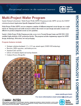
Sandia’s Multi-Project Wafer (MPW) Program provides MPW services for radiation-hardened Application-Specific Integrated Circuits (ASICs).
MPW services integrate a number of different integrated circuit designs on a single reticle set. Sharing mask and wafer resources reduces the overall cost per design and makes it more cost effective to produce integrated circuits in low quantities.
Sandia National Laboratories’ Multi-Project Wafer Program offers access to its Trusted Design Center and high-reliability ASIC production facility. The program includes engineering support for MPW design, technology, fabrication, test and packaging, all in a trusted environment.
The MPW Program will be available to external customers beginning in 2010.
Program features include:
• Strategic radiation-hardened 3.3V, 0.35μm mixed-signal CMOS-SOI technology.
• Resistors, MIM capacitors, and diode passives.
• Standard Cells and IOs.
• Library of common digital and analog elements.
• Cadence Process-Design Kit.
Sandia National Laboratories’ structured Application Specific Integrated Circuit (ASIC) provides a radiation-hardened, via-configurable implementation platform with ASIC-like performance. Structured ASICs enable rapid turn-around, lower Non-Recurring Engineering (NRE) and development costs. Pre-qualified base arrays reduce development risk, while open architecture minimizes Diminishing Manufacturing Sources (DMS) issues. Enables safe, secure, user-defined trusted hardware, and the regular, fabric-like structure enhances verifiability of trusted parts.
Special Features
- Metal-via configurable, fabric-like structure using ViASIC™ ViaMask Technology.
- Four Power-Quadrants with specialized interface circuits that allow up to four independent power supplies for power sequencing and redundancy operations.
- Unused transistors and circuits are isolated from power and ground to minimize power consumption, static current and photocurrent.
- On-package decoupling capacitors.
Applications include:
- Command & Control
- Instrumentation
- Sensor Monitoring
- Obsolescent Parts & FPGA Emulation
- Rad-hard environment operations
- High-Reliability Systems
Sandia National Laboratories has historically focused on high-reliability custom solutions for high-consequence applications. Today Sandia is a DoD Category 1A Accredited Supplier of both “trusted design and foundry services” optimized for high-mix low-volume custom radiation-hardened, digital, analog and mixed-signal ASICs. With in-house capabilities in packaging, test, failure analysis and reliability, Sandia offers a total supply-chain solution for high-reliability custom microelectronics for expanding national security applications.
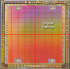
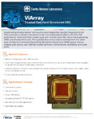
Eiger Digital Rad-Hard ViArray
Digital Functions
• 276K Gates
• 368Kb Dual-Port SRAM
• 384Kb Configurable ROM
• 4 Oscillators
• 4 Phase Lock Loops
• 4 Power Supply Monitors
• 4 Power Partitions
• Isolated Unused Circuits
• 239 Configurable I/Os
• (PCI compatible)
• 8 Pairs LVDS I/Os
Whistler Mixed-Signal Rad-Hard ViArray
Analog Functions
• 2 Oscillators
• 2 Phase Locked Loops
• 4 Power Supply Monitors
• 4 Bandgap References
• 2 Chopper Bandgap/Bias
• 5 High Side Current Monitors
• 4 Low-Speed A-D Converters
• 4 Pipeline A-D Converters
• 8 D-A Converters, 8-bit
• 8 Multiplexers, 32:1
• 2 Temperature Sensors
• 64 Comparators
• 48 Amplifiers
• 128 Analog Switches
• 1 Analog Transient Recorder
Digital Functions
• 138K Gates
• 184Kb Dual-Port SRAM
• 192Kb Configurable ROM
• 4 Power Partitions
• Isolated Unused Circuits
• 239 Configurable I/Os (PCI compatible)
• 4 with High/Low Voltage Analog Inputs
• 8 Pairs LVDS I/Os
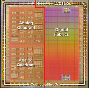
Technology
• 3.3 v
• 0.35 µm
• SOI CMOS
Package options
• 400 pin plastic BGA 27×27 mm
• Other package options in development
III-V Compound Semiconductor Fabrication
Sandia provides custom compound semiconductor microelectronics solutions. These include surface-normal and guided-wave optoelectronics, optical and microwave microelectromechanical devices and systems, compound semiconductor epitaxy, and rad-hard and high-power density microelectronics. Examples of device and circuit technologies we have researched, developed and delivered include:
• A wide variety of specialty semiconductor lasers
• Integrated VCSEL-RCPD circuits (vertical-cavity surface-emitting lasers, resonant-cavity photodiodes)
• Photonic integrated circuits (GaAs, InP)
• Planar lightwave circuits (SiON materials set) such as various optical guided-wave filters and switches
• Optical data links
• Micromirror arrays and subsystems for switch matrices and adaptive optics
• Radio-frequency switches and networks that include phase shifters and tunable filters
• Power amplifiers
• Low-noise amplifiers
• Rad-hard heterojunction bipolar transistors
• High-electron mobility transistors
(1) Amplifiers
(2) Heterojunction Bipolar Transistor (HBT)
(3) Optoelectronics/VCSELs

Sandia National Laboratories’ Metal Micromachining Program specializes in the fabrication of small innovative devices. Its technologies have been applied to diverse fields including quantum computing, photovoltaics, kilohertz waveguide development, nuclear magnetic resonance imaging, and phase contrast imaging. With expertise in the fabrication of thick, high aspect ratio uniform metal and metal alloy structures too small for traditional machining, the Program maintains a suite of tools and capabilities that transform big ideas into little devices.
For more information: Metal Micromachining Program
The Sandia Ultra-planar, Multi-level MEMS Technology 5 (SUMMiT VTM) Fabrication Process is a five-layer polycrystalline silicon surface micromachining process (one ground plane/electrical interconnect layer and four mechanical layers).
Motivation
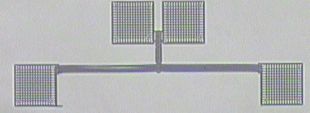
While the devices made possible by fabrication using the four-layer SUMMiTTM Process are truly complex, there is further benefit in providing yet another layer of mechanical polysilicon. For example, with the SUMMiT VTM Process, more advanced systems can be created on moveable platforms (Figure 1). Much taller devices can be made (up to 12 microns high), making possible greater stiffness and mechanical robustness in the devices (Figure 2). The additional height can also be used to increase the force produced by actuators (Figure 3). The design flexibility in a five-layer technology is truly enormous – devices for applications that have not yet been imagined are now a possibility.
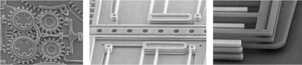
Figure 1. Meshing gears on a moveable platform.
Figure 2. Laminated support springs containing only three mechanical layers result in more than 2 orders of magnitude greater out-of-plane stiffness in comparison to that of a single mechanical layer.
Figure 3. A laminated comb actuator results in nearly five times the electrostatic force of a single level actuator.
Fabrication
As with the SUMMiTTM Process, the SUMMiT VTM Fabrication Process is a batch fabrication process using conventional IC processing tools. Using this technology, high volume, low-cost production can be achieved. The processing challenges, including topography and film stress, are overcome using methods similar to those used in the SUMMiTTM Process: topography issues are mitigated by using Chemical-Mechanical Polishing (CMP) to achieve planarization, and stress is maintained at low levels using a proprietary process.
MEMS are also produced in the SUMMiT VTM Fabrication Process by alternately depositing a film, photolithographically patterning the film, and then performing chemical etching. By repeating this process with layers of silicon dioxide and polycrystalline silicon, extremely complex, inter-connected three-dimensional shapes can be formed. The photolithographic patterning is achieved with a series of two-dimensional “masks” that define the patterns to be etched. The SUMMiT VTM process uses 14 individual masks in the process, approximately the same quantity as in many CMOS IC processes.
Testimonials…
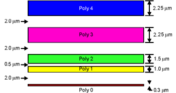
In relation to the SUMMiT V fabrication of a dual backplate capacitive MEMS Microphones, Dr. Toshi Nishida of the University of Florida said “We have developed a MEMS microphone using Sandia’s Ultra-planar, Multi-level, MEMS Technology (SUMMiT V) fabrication process. The microphone is a dual backplate capacitive microphone that may be operated in either open loop or closed loop mode. electrostatic force feedback. The microphone consists of a diaphragm and two porous backplates, one on either side of the diaphragm. The SUMMiT V fabrication process is unique in that it can meet the fabrication requirements of this project. All five layers of polysilicon are used in the fabrication of this device; Poly 0 is used for electrical connections, Poly 1 and Poly 2 are combined to form the lower backplate, Poly 3 is used for the diaphragm, and Poly 4 is used for the top backplate. The SUMMiT V process provides compliant mechanical layers that are ideal for the construction of the microphone’s diaphragm, especially due its use of chemical mechanical polishing to provide extremely flat structural layers and uniform spacing between the layers. The microphone demonstrates a flat frequency response, a linear response up to the designed limit, and a sensitivity which is close to the designed value. Sandia National Labs has been an essential partner in this project by providing access to and training for the SUMMiT V process.”
Fairchild Semiconductor has said, The Summit™ technology is well recognized as the leading micromachining process for MEMS devices. “Network Photonics has worked with Sandia’s Summit IV™ technology and found the process to be a stable, well-characterized, platform for producing MEMS-based optical switching solutions,” said Andy Goldstein, vice president of engineering for Network Photonics. “This process meets the high levels of reliability and performance Network Photonics requires for its customers.” Fairchild is already in volume production of MEMS devices at its 6 inch wafer facility in South Portland. “We are pleased to see a company of Fairchild’s stature become a provider of our Summit IV™ technology,” said Jay Jakubczak, Sandia deputy director for Defense Programs Microsystems Application. “It has been a goal of our MEMS effort to make our technology available for broad commercial applications and the relationship with Fairchild is an important step in achieving that goal.
Sandia has been providing access to the Summit™ Technology through its SAMPLES | Prototyping program that supports small quantities of MEMS devices. Making the Summit™ processing technology available through Fairchild significantly increases the volume of MEMS devices that can be manufactured.
Sandia SUMMiT™ V MEMS Devices launched aboard NASA ST5 Micro-Sats
A constellation of 3 Micro-satellites were ejected at 3 minute intervals during a launch aboard a Pegasus XL rocket on 22 March, 2006. The spacecrafts’ orbit is a “string of pearls,” in a near-Earth polar elliptical orbit that will take them from approximately 300 kilometers (190 miles) to 4,500 kilometers (2,800 miles) from the Earth.
This was part of NASA’s Space Technology 5 (ST5) mission to explore concepts of building and operating miniaturized micro-sats. ST5 is the first step in developing missions of tens or hundreds of small spacecraft that would look at phenomena such as space weather.

The ST5 micro-sats will explore the Earth’s magnetic field using highly sensitive magnetometers, in addition to evaluating 10 technologies applicable to the development of micro-sats. One of the technologies being evaluated is Variable Emittance techniques for satellite thermal control which operates by either absorbing or reflecting heat. Two of the three satellites each contain 90 sq. cm of MEMS variable emittance louvers which were designed and fabricated at Sandia using the SUMMiT V™ (Sandia Ultra-planar, Multi-level MEMS Technology 5) MEMS fabrication technology. Sandia delivered the SUMMiT™ wafers to the Applied Physics Lab in fall 2001 for further processing and system integration as part of the joint development program with Johns Hopkins University Applied Physics Laboratory and NASA Goddard Spaceflight Center . The thermal performance of the variable emittance louvers will be evaluated during the 3 month mission.
“This is the first time a fully space-qualified device of this type has ever been flown, and the first to be flown on the outside of a satellite,” says Ann Darrin, APL’s Vari-E program manager, who explained that the devices underwent the same rigorous tests that all space products undergo prior to launch. “It’s also the first demonstration of MEMS technology used to actively control temperature.”
More information
In the last decade, devices manufactured with the SUMMiT ™ technology have demonstrated the capabilities of polysilicon surface micromachining. Currently Sandia is working on enhancements to this technology that utilize additional structural layers of silicon nitride to enable Microfluidics and BioMEMS applications. The addition of the silicon nitride layers allows the fabrication of microfluidic flow channels that are optically accessible (allowing observation) and insulating (allowing the placement of polysilicon electrodes at arbitrary locations in the flow channels). The goal of this effort is to provide functionality that is not feasible with other microfabrication technologies. The enhancements build on the key features of surface micromachining: manufacturability and compatibility with CMOS processing, which allow us to leverage the investment already made in microelectronics processing technology. Examples of devices fabricated using this technology include pumps, valves, and a cell manipulator.
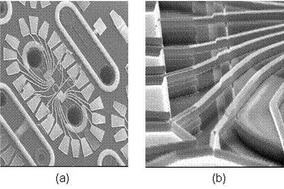
(a) A flow channel with electrodes for creating/sensing electric and magnetic fields. Electrodes with varying shapes and spacing allow creation of almost any arbitrary field inside the channel for driving separations and in-channel synthesis.
(b) Close-up SEM of polysilicon electrodes formed around the silicon nitride channcel structure.
Figure 4. Red blood cells flowing through the cellular manipulation device
Sandia designs, characterizes and delivers miniaturized, reliable RF MEMS components and systems such as filters, switches, and oscillators that provide differentiating capabilities to Sandia system groups impacting national security and nuclear weapons.
For more on RF MEMS see the MicroElectroMechanical Systems (MEMS) page.
Aluminum Nitride RF MEMS Resonators
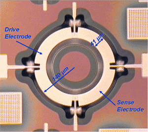
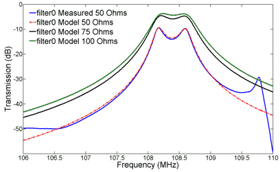
Sandia has developed an aluminum nitride (AlN) process for fabricating RF MEMS micro resonators at frequencies ranging from 1 MHz to 3 GHz. This process uses the same equipment and materials that were developed to fabricate FBARS (film bulk acoustic resonators), which are widely used to implement cellular phone duplexers and filters at 1.9 GHz. Like FBARS, the piezoelectric transduction mechanism of these resonators allows the realization of low insertion loss filters. Unlike FBARS, Sandia’s AlN process allows resonators at any frequency between 1 MHz and 3 GHz to be fabricated on the same wafer because the resonant frequency is determined lithographically. The AlN resonator process also includes Sandia’s unique molded tungsten (W) capabilities. Incorporation of W into the AlN process eliminates the need for resonators that are suspended above the substrate by quarter-wave beams. It is this technology that allows the scaling of AlN resonators into the GHz range without introducing spurious modes, reductions in quality factor (Q), and with acceptable power handling for both the transmit and receive paths in full-duplex radios. This technology is most suited for realizing resonators from 1 MHz to 3 GHz, with Q’s approaching 5000, and impedances less than 300 Ohms.
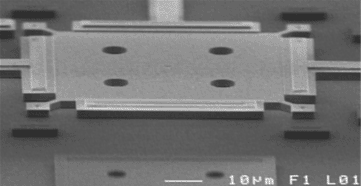
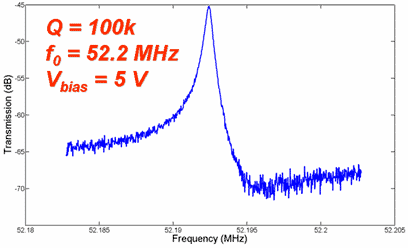
Narrow-gap Polysilicon RF MEMS Resonators
A polysilicon MEMS resonator process has been developed at Sandia for the fabrication of high-Q oscillator references and intermediate frequency (IF) filters. This process can achieve electrode-to-resonator gaps less than 100 nm, which is needed to reduce the impedance of capacitively transduced devices. While high frequency resonators can be implemented in this process, it is best suited for fabricating resonators below 200 MHz because the impedance levels are significantly lower at these frequencies. Advantages of these polysilicon resonators when compared to microfabricated piezoelectric resonators include much higher Q (> 60,000), low drift, tunability, and low vibration sensitivity. These properties make polysilicon µresonators ideal for implementing miniature oscillators and IF filter banks for RF MEMS applications.
RF MEMS Reliability
Through measurement, characterization and analysis, we provide customer feedback to improve operation, performance and reliability of MEMS components, specifically RF switches. We have testing capabilities at the DARPA standard for MEMS switches (RFMIP) of 10 GHz. We have conducted environmentally controlled studies of switch performance and lifetimes at temperatures ranging from -15C to 75C, including cycling. Through failure analysis, we have worked with our customers to enhance understanding of operation, mechanically and electrically. We have performed tests to understand contamination issues that have caused early failures. We are investigating functionality and performance of RF sensor applications to monitor corrosion and to predict critical component failures. By utilizing knowledge of MEMS and by providing unique measurement and characterization capabilities, we can be an integral part of any MEMS project.
Sandia develops High-performance passive waveguide technologies for sensing and communication applications critical to our nation. Several planar lightwave circuit (PLC) technologies have been developed at Sandia that are ideally suited to applications where low-loss waveguides, thermo-optic switches, and high-Q resonators are needed.
Sandia’s strengths in modeling, design, fabrication, and testing have successfully produced ultra low loss, planar lightwave circuit (PLC) technologies with record low loss and high manufacturability in a fully operational CMOS fabrication line.
Figure 9. Lateral mode interference (LMI) 3 dB splitter: simulation (top left) and fabricated device (top rit), measured results (bottom)
Our Low Loss Silicon Nitride waveguide technology consists of a patterned Silicon Nitride optical waveguide core sandwiched between silicon dioxide cladding materials fabricated on a standard 6-inch silicon wafer. Process development efforts have demonstrated a polarization maintaining, single mode, optical waveguide, with record low attenuation of 0.1 dB/cm.
The index of refraction difference between the silicon nitride core material and the silicon dioxide cladding (2.01 vs. 1.45) makes this an ideal material system for designing small radius bends and complicated device geometries. Polysilicon heaters, metallized bondpads and mode expanding taper interfaces have been monolithically integrated and delivered with this principal PLC technology, and future micro-system integration efforts are under way for multi-material, multiple technology integration. For applications, such as resonant ring gyros where lower attenuation losses are desirable, accelerated process development is currently being executed to produce a (SiON/SiO2) technology with an attenuation goal of 0.05dB/cm or less.
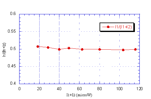
Evanescent Wave Microring Biochemical Sensor
The transmission of a waveguide coupled high-Q microring resonator is sensitive to the perturbation of its optical path. A slight change of either the mode index or the microring physical size can cause a significant change in the transmission near its resonances. The high-Q integrated microring resonators can be used as ultra sensitive photonic transducers for a variety of sensor applications such as biochemical, gravity, acceleration, pressure, and electromagnetic sensing.
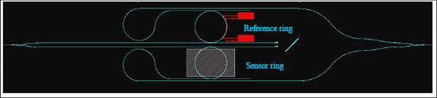
Microring biochemical sensor with a reference microring resonator
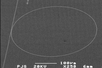
Fabricated Microring
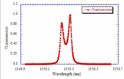
Ring resonance for water
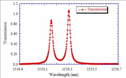
Ring resonance for methanol
Based on the evanescent wave and the high-Q microring resonator, Sandia demonstrated a liquid phase chemical sensor that can sense the small change of index of refraction of liquid phase chemicals. The on-chip evanescent wave microring biochemical sensors have the intrinsic capability and potential for large array multi-channel device integration and low cost mass production. Two parallel rings are used in transmission with separate input and output waveguides. One ring is the sense ring while the other is a reference ring embedded in a thick cladding and is not exposed to any biochemical liquids. On the top of the sense ring a window is etched to thin the cladding layer so that the evanescent wave can penetrate through it to reach the liquid. The input light is first coupled into the input waveguide and then split equally into two waveguides which are coupled to the reference ring and the sense ring. Two additional waveguides are used to couple the light out from the reference ring and the sense ring. A beam combiner is used to combine the light from the rings. As the input wavelength is scanned, we expect to see two distinct transmission resonances, one for each ring. The difference between these resonance frequencies is a direct measure of the refractive index of the liquid in the sense region.
Sandia has developed multiple passive waveguide technologies in combinations of the following materials:
• Silicon Dioxide
• Doped Silicon Dioxide
• Silicon Nitride
• Silicon Oxynitride
• Silicon on Insulator
• Polysilicon
The oxide molded tungsten process can be used for the fabrication of complex multilevel structures which can be relatively thick. The steps in the process are the deposition of a sacrificial oxide, patterning etching of the oxide, filling of the resulting mold by a blanket film of tungsten using chemical vapor deposition, and then removal of excess tungsten and planarization through chemical mechanical polishing. We have termed this process MOLTUN™ which is short for Molded Tungsten. This process has been used to demonstrate complex multilevel devices such as micro-mass-analysis systems up to 25 microns thick and novel latching relays which take advantage of the inherent tensile stress of the tungsten. Benefits of this process include high Z stiffness, high force actuation, high capacitance, maintenance of planarity and reduction or compensation for stress. Possible applications for MolTun™ include actuators, miniature mass analyzer, adaptive optics, and inertial sensors. Using current microfabrication process and materials it is possible to fabricate a wide very large variety of useful devices.
Micro-Mass-Analysis Systems Applications
MolTun™ has been used in Micro-Mass-Analysis Systems resulting in large (up to 106) arrays of cylindrical ion traps consisting of 4 separate electrode layers each separated by gaps. The devices are thicker than those achievable using traditional surface micro-machining and are far more complex than those achievable using deep trench etching. The pictures below show the highly complex W parts. The thickest parts fabricated for this project had ~14 layers of tungsten, 8 of which went into the fabrication of the ring electrode. The total thickness of the structures was ~25 microns. This is considerably thicker than typical polysilicon micromachined structures.
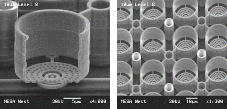
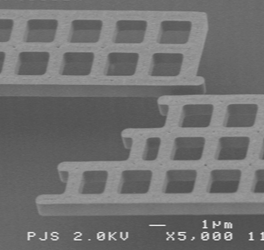
SEM micrographs of partially completed micro-mass-analysis systems.
Micro-Latching Relays
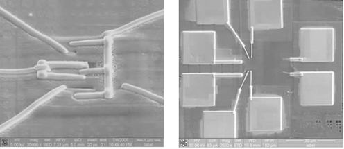
MolTun™ has also been used in micro-latching relays in which the design takes advantage of the internal tensile stress of the released W. The micro-mass analysis system is mechanically a static device and the residual tensile stress of the W is dealt with by simply anchoring the array firmly to the substrate. In the micro-latching relay this tensile stress is critical to the functioning of this mechanical device. The general design is based on having two pairs of opposing thermal actuators. The first picture below shows a typical released chevron type thermal actuator fabricated in the MOLTUN™ process. Initially the arms of the thermal actuator were at 4 degrees to the line between the pad centers. Upon release, the residual tensile stress of the W has pulled the arms of the thermal actuator straight. Our results show that the displacement can be considerable, tens of microns depending on geometry, and that angles greater than 4 degrees would be required to completely “relax” the tensile stress associated with these released W devices. In our latching relay design we place two orthogonal pairs of identical thermal actuators in opposition to each other, as seen in the second picture below. Since the system is symmetrical the overall displacement of the central shuttle is zero at rest. Passing a current to heat one of the heater arms causes it to expand and allows the opposing thermal actuator to reduce its internal stress by pulling the central shuttle towards it. The forces exerted in this design are always “pulling” in nature. In a conventional thermal actuator design the force generated is typically “pushing” in nature and when the force becomes sufficiently large the thermal actuator buckles and it becomes impossible to increase the actuation force. In our “pulling” W design it is impossible for the system to relax the force exerted by deforming into a buckling mode.
Top view optical micrograph of a released chevron thermal actuator fabricated using the MOLTUN™ process. Initially the arms of the thermal actuator were at 4 degrees to the line between the center of the two anchor pads. The residual stress in the W resulting from the thermal expansion mismatch between the Si and the W is sufficient to pull the arms straight.
Oblique angle SEM micrograph showing the latching relay design developed for the MOLTUN™ process. In this design two pairs of identical thermal actuators are arranged opposing each other and attached to each other through a suspension and a suspended plate. Since the system is symmetrical the overall displacement of the central shuttle is zero. Actuating one of the chevron thermal actuators allows the opposing thermal actuator to relax and pull back. Having two sets of orthogonal pairs of actuators enables X-Y translation of the central shuttle.
The opposing thermal actuation mechanism translates the top portion of the shuttle so that the two teeth engage. Once the teeth are engaged the actuation mechanism can be powered down and the structure remains latched in position. Two such structures electrically connect two pads through the moving shuttle.
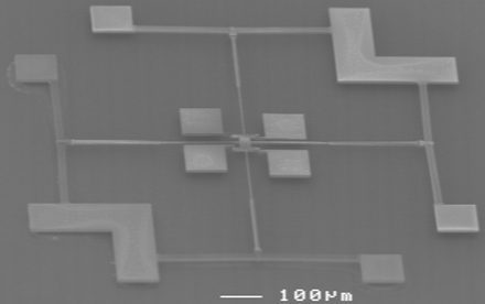
MEMS devices are created with processing tools and infrastructure very similar to that used to fabricate conventional integrated circuits. Our advanced MEMS and integrated MEMS (IMEMS) are created in the Silicon Fab (SiFab), part of the Microsystems Engineering Sciences and Applications (MESA) Complex, located at Sandia National Laboratories. The SiFab is a world-class fabrication facility dedicated to providing development and engineering capabilities to support industry, government, and other programs of national interest.
Microsystems Engineering Sciences and Applications (MESA) Complex
Sandia National Laboratories (SNL) has invested heavily in the Microsystems and Engineering Sciences Applications (MESA) facility located in the heart of a multi-laboratory complex. Trusted custom fabrication of silicon and radiation-hardened process technologies for digital, analog and mixed signal ICs is currently available through MESA, which delivers production micro-electronics components to support special DOE and DOD programs. The MESA Complex is designed to integrate the numerous scientific disciplines necessary to produce functional, robust, integrated microsystems and represents the center of SNL’s investment in microsystems research, development, and prototyping activities. This suite of facilities encompasses approximately 400,000 square feet and includes cleanroom facilities, laboratories and offices.
MesaFab
The SiFab has 34,500 square feet of clean room space and state-of-the-art equipment for processing wafers up to 6 inches in diameter. Class 1 clean room processing (less than 1 particle 0.5 micron or larger per cubic foot of air) is available in bays totaling over 12,000 square feet of space.
The flexible layout also allows the SiFab engineers to work efficiently on many projects that require some degree of isolation, such as benchmarking of advanced process tools, development of state-of-the-art micromachining techniques, and research into materials science and surface chemistries for advanced silicon technology development.
The SiFab’s professional staff includes a core of Ph.D. and Master’s level engineers and scientists experienced in a broad range of disciplines including microelectronic and micromachining process development, equipment design, materials engineering, device physics, chemical engineering, sensor science, circuit design, computer science, failure analysis, reliability physics, and industrial hygiene.

The MESAFab complex develops and maintains core semiconductor processing capabilities and capacity that enable our customers to build differentiating Microsystems products. Two unique facilities are co-located within the 65,000 square foot MESAfab complex including: (1) a 34,500 square foot Silicon Fab for 6-inch silicon wafer processing with Class 1 bays and (2) a 30,400 square foot MicroFab with Class 10 and Class 100 bays for compound semiconductor material processing and silicon wafer post-processing.
The Silicon Fab has processing expertise in both CMOS and MEMS technologies. Over 150 equipment sets are maintained, supported and operated 24 hours per day, 5 days a week (3 shifts). Both processing and maintenance expertise are staffed on all 3 shifts. We offer unique prototyping capabilities. We are capable of producing full flow production lots with quick turnaround time as well as performing flexible process development and unique research and integration opportunities.
The III-V compound semiconductor and silicon wafer post processing Fab has expertise on GaAs,InP processing and many other semiconductor systems. Silicon post processing is used in micro-machine release, photovoltaic devices, hetro-integration, 3d device stacking, and a host of technologies. We staff and support processing and maintenance for 2 shifts 5 days a week. The unique capabilities of this fab combine with our expertise in novel integration schemes to deliver state of the art research and small volume production.
Packaging
Packaging and assembly involves interconnecting ICs and/or other components to a plastic or ceramic substrate, and subsequently integrating that package into a system. Over the span of four decades, the Microsystems Integration Department has developed core competencies in microsystems packaging and assembly. Strategic partnerships within Sandia, and with national laboratories, universities, commercial packaging houses, and private industry enable the development and implementation advanced microsystems packaging solutions with the greatest value to our customers.
Packaging Technologies:
• Hermetic ceramic and plastic high reliability packaging (all standard configurations)
• RF and optoelectronics packaging
• MEMS packaging
• Flex and surface mount assembly
• Rapid hybrid microsystems prototyping
• Ultra-miniaturization (3-D packaging and 3-D Integration)
Sandia has the ability to prototype, and to provide quick turn plastic and ceramic packaging and assembly for trusted applications.
Capabilities include:
Seal and Encapsulation
- Hermetic ceramic packaging
- Solder lid seal
- Parallel seam sealing
- Glob top
- Dam and fill
Packaging and Assembly Design/Development
- Package design and selection (ceramic and plastic substrates)
- Thermal management
- Materials selection and evaluation
- Packaging and assembly process development
- Full custom microsystems integration
Custom Packaging and Assembly
- Multi-chip modules
- Thermo-compression bonding
- Die-to-die, wafer-to-wafer, and die-to-wafer.
- MEMs packaging and assembly
- RF assembly
- Optoelectronic assembly
- Flex circuit assembly
- Surface Mount assembly
- Rework and repackaging
Dicing
- Die singulation
- MEMS dicing
- Dicing of
- Si, glass, quartz, and various ceramics (alumina, LTCC, AlN, etc.) and organics
- Up to 200 mm wafers
- Thinned wafers
- Multi-project wafers
Die Attach
- Manual and automated, precision die placement
- Conductive and nonconductive organic (epoxy) die attach materials
- Eutectic die attach
Wire Bonding
- Manual and automated wire bonding
- Aluminum and gold wire
- Wedge and ball bonding
- Fine pitch (down to 50 um)
- High wire count
- Wire bonding to ceramic, organic, metal packages
Flipchip Assembly
- Eutectic and high Pb solders
- Au stud bumping (wafer or die)
- Plastic and ceramic substrates
- Precision underfill dispensing
Testing and Assurance
The Microsystems Integration and Failure Analysis departments collaborate closely to qualify and test products to evaluate performance and reliability.
Capabilities include:
Die Sorting and Inspection
- Die and wafer tracking
- Laser marking
- Optical Inspection
Test Performance and Reliability
- Environmental testing
- HAST (highly accelerated stress testing)
- HALT (highly accelerated lifetime testing)
- Long-term dormant storage
- Temperature cycling
- Nondestructive testing
- CSAM (C-mode scanning acoustic microscopy)
- Real-time x-ray imaging
- 3D X-Ray Tomography
Thermal Management
- Thermal Simulation and modeling
- Thermal imaging
Design for Test and Manufacturability
- Design-for-Test (DFT)
- Scan/ATPG Insertion
- Logic and Memory Built-in Self Test (BIST)
- Insert Test Interfaces (JTAG)
Radiation Hardening or Rad-Hard is an essential service that Sandia National Laboratories can perform. Rad-Hard electronic components are a vital link for systems that operate in space, high altitude, defense systems or in close proximity to nuclear reactors. Due to the ionization effect that radiation produces, hardening provides that additional level of protection that is necessary in extreme environments. Sandia National Laboratories offers solution to tomorrow’s challenges by providing rad-hard services such as:
- Design and Layout
- System Modeling
- VHDL and Verilog
- Rad-Hardened ASICS
- Optical Technology
- Nano Technology
- Testing and Assurance
Sandia Radiation Physics Total Ionizing Dose Testing
Gamma ray Radiation Sources
The Radiation Physics, Technology, and Assurance department at Sandia National Laboratories maintains 4 gamma ray radiation sources, including two 60Co sources and two 137Cs sources. These sources are located on-site in the department’s laboratory space in New Mexico, and are routinely used for radiation qualification of Sandia and commercially fabricated ICs, as well as basic studies of the physical mechanisms responsible for radiation effects in semiconductor devices. Radiation testing in these cells requires that the parts to be tested are packaged and mounted on circuit boards. For low-dose-rate irradiations, the department uses three J. L. Shepherd radiation sources shown in Figure 1. The large irradiator in the foreground is a 60Co radiation cell capable of dose rates ranging from < 0.1-30 rad(SiO2)/s. This cell is primarily used for qualification testing and basic studies of radiation damage mechanisms in electronic components at low to intermediate dose rates. In the background in Figure 1 are two identical 137Cs radiation cells used for studies and qualification testing of electronic components at low dose rates (< 0.001-5 rad(SiO2)/s).
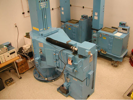
Figure 1. Sandia Radiation Physics department Shepherd 60Co and 137Cs gamma radiation sources. Figure 2 shows the MDS Nordion Gammacell 220 radiation cell operated by the department. This source is used for qualification testing of electronic components per MIL-STD 883, TM 1019, which requires testing to be performed in the dose rate range of 50-300 rad(SiO2)/s. The current maximum dose rate achievable in this radiation cell is ~60 rad(SiO2)/s.
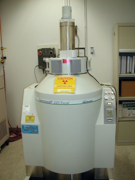
Figure 2. MDS Nordion Gammacell 220 radiation cell.
X ray Radiation Sources
The Radiation Physics, Technology, and Assurance department at Sandia also maintains three Aracor 4100 X ray irradiators. These irradiators use X ray tubes to irradiate the device under test, and are especially well suited to wafer-level radiation studies. Figure 3 shows one of these irradiators, which consists of a cabinet in which the x ray tube is located, as well as a probe station which is used for wafer-level irradiation. Although these irradiators are primarily used for wafer-level radiation testing of products and test structures for technology development and process monitoring of wafers fabricated in Sandia’s own fabrication facility, they can also be used to irradiate parts that have already been packaged.
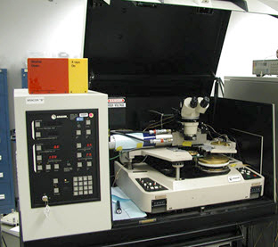
Figure 3. Aracor wafer-level x ray irradiator.
Sandia Radiation Physics Single-Event Effects Testing
Broadbeam Heavy Ion and Proton Accelerators
Single-event effect testing is typically performed off-site at large heavy ion or proton accelerator facilities such as the Brookhaven National Laboratory’s Tandem van de Graaff heavy ion accelerator, the Texas A&M heavy ion cyclotron, and the Indiana University or TRIUMF proton cyclotrons. These facilities are all run as user facilities and are routinely available for parts characterization and evaluation. An example of such a facility (in this case the Brookhaven Tandem) is pictured in Figure 4. In such facilities the device under test is typically placed at the end of the beam line and is subjected to energetic particle irradiation while any anomalous behavior is recorded. The resulting measured single-event upset cross section curve is used in conjunction with the expected radiation environment to calculate the predicted upset rate for a given application. The Radiation Physics, Technology, and Assurance department conducts several remote-site radiation tests per year and is intimately familiar with procedures for performing testing at all of these radiation facilities.
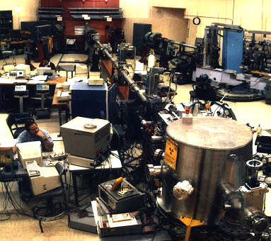
Figure 4.Brookhaven National Laboratory Tandem van de Graaff heavy ion accelerator.
Sandia Focused Heavy Ion Microbeam
Broadbeam experiments are typically used for heavy ion qualification testing, but an unfortunate drawback of such testing is that no direct positional information on the device response is obtained- only the aggregate response of the entire chip. For diagnostic purposes it is often desirable to acquire positional information. Such information can be gained through the use of a focused ion beam. Sandia operates a focused ion microbeam facility in a sister organization to the Radiation Physics, Technology, and Assurance department. This facility, pictured in Figure 5, consists of a magnetic lens that focuses the beam exiting a van de Graaff accelerator, and an electrostatic beam scanning capability that allows the resulting submicron ion beam spot to be scanned across the surface of the device under test. By noting the position of the beam corresponding to an observed anomaly in the device being tested, and correlating this position to the circuit design via the layout mask, the precise location and cause of the anomaly can be determined.
Radiation Physics Device and IC Test Capabilities
IC Testers
Certimax 105 Portable IC testers, 125 MHz with 128-pin capacity, two units can be connected for 256 pins. HP 82000 Digital ASIC testers, two portable D50 chassis with 48-pin capacity and 128-pin capacity, and one fixed D100 chassis with 256-pin capacity. Analog Devices LTS2020 Analog tester for performing parametric and functional tests on bipolar linear ICs.
Parametric Testers
HP 4062UX Parametric Test Systems interfaced to Aracor 4100 X-ray test system. HP 4145/4156 Semiconductor Parameter Analyzers with high voltage and charge pumping capabilities. National Instruments PXI Portable Parametric Test System.
Other Test Equipment
Automated wafer probe, multiple ovens for annealing studies, thermally stimulated current test setup, and comprehensive electrical test equipment such as power supplies, oscilloscopes, switch matrices, etc.
Silicon Photonics Fabrication
Sandia’s Silicon Photonics devices are fabricated in the SiFab at Sandia’s Microsystems and Engineering Sciences Applications (MESA) Complex, leveraging our production equipment and capabilities for radiation-hardened CMOS integrated circuits. We have developed a Silicon Photonics Design Manual that allows designers to create photonic prototypes.
In 2014, we successfully completed our first multi-user project wafer in collaboration with NSF funded Center for Integrated Access Networks (CIAN) where 5 university groups submitted designs and received working devices.
Validation
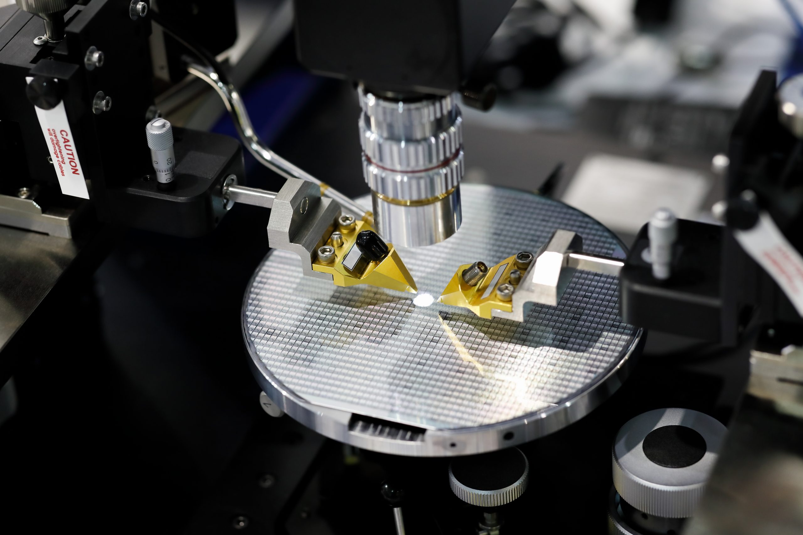
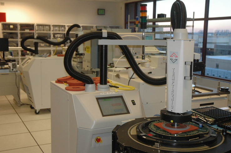
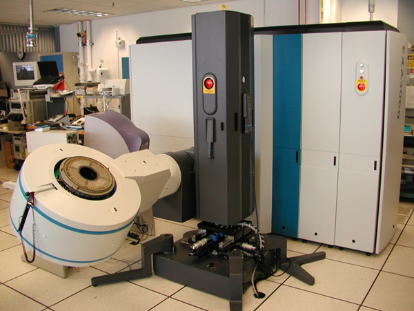
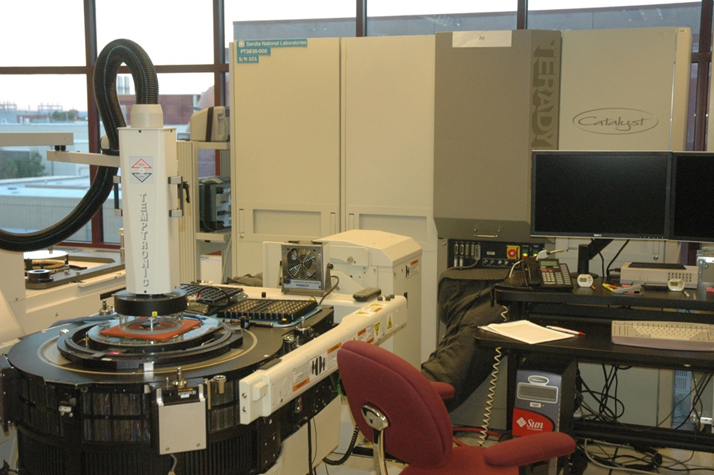
Sandia’s experienced in-house Test Engineering group develops custom test programs for electrical test of digital, analog and mixed signal semiconductor devices. The group performs semiconductor wafer-level electrical testing of individual dice, as well as packaged part electrical testing across the full specified temperature range. The group performs prototype, characterization and production testing of custom ASIC devices and commercial off-the-shelf devices (COTs).
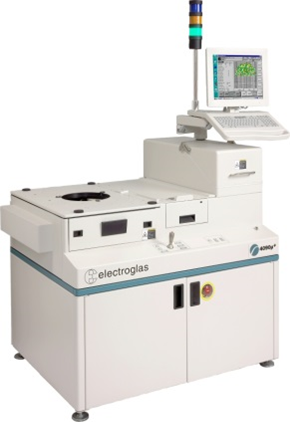
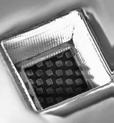
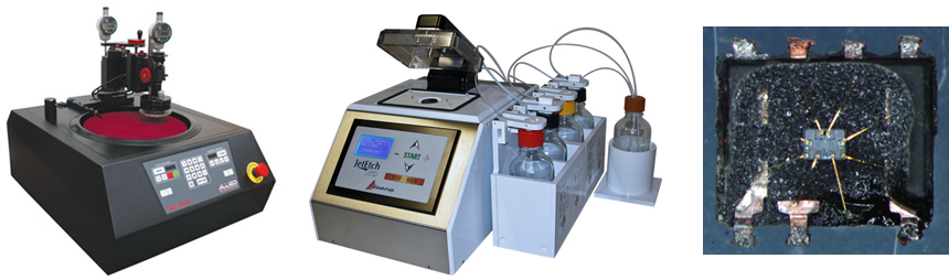
(left)EG4090u+: Wafer Prober capable of handling 6” and 8” semiconductor wafers; interfaces to Automated Test Equipment (ATE) for electrical testing.
(right)Temptronic Thermostream: Provides capability to test devices across the full Military Standard temperature range.
Digital Automated Test Equipment
- EXA3000
- 496 Digital Channels
- 8 LVDS Pairs
- 300MHz Maximum Frequency
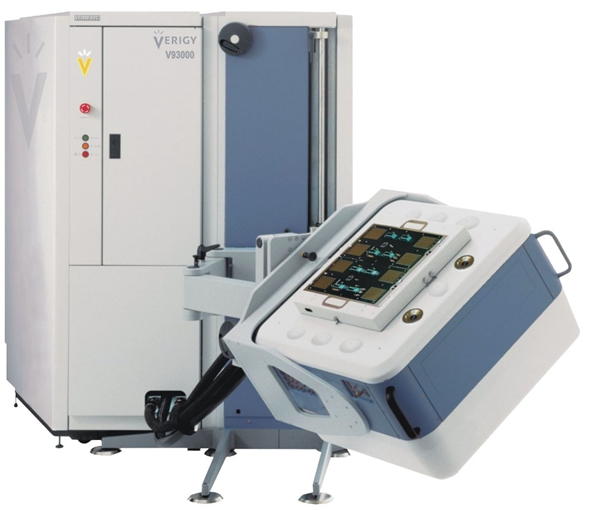
Mixed Signal Automated Test Equipment
- Teradyne Catalyst
- 384 Digital Channels
- 400MHz Maximum Frequency
- Analog Source and Capture Instrumentation
- Advantest V93K
- 512 PS800 Digital Channels
- 200MHz (<=3V) 400MHz (<=1V) Maximum Frequencies
- 96 PS3600 Digital Channels
- 1.6GHz Maximum Frequency
- Analog Source and Capture Instrumentation
Burn-in
Burn-in is a process where semiconductor components are exercised prior to being placed into service. This method of testing forces certain failures to occur under known environments and test conditions. The intention is to detect components that would exhibit a high failure rate and ensure they are not put into service. Understanding the performance capabilities of the semiconductor components enables engineers to optimize functionality during service.
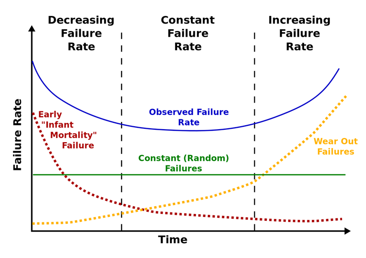
Typical bath-tub curve depicting early or “infant mortality” failures followed by the constant or “random” failures, then the increasing wear out failures over time.
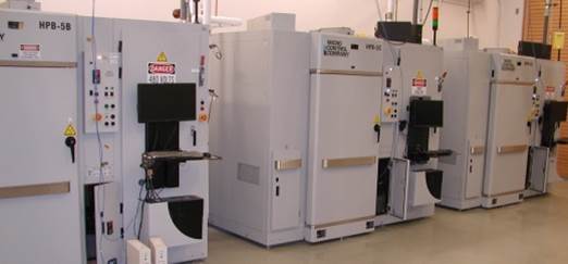
At Sandia, burn in ovens used to electrically test packaged devices at elevated temperatures. Three MCC HPB5 ovens and a pre-screen station are used for Diagnostics and burn in.
Reliability
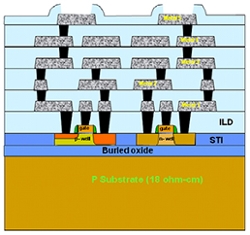
Ultra-high reliability is critical for CMOS7 technology and other NW parts. It is achievable only through tight manufacturing quality control, circuit design that ensures margins for component aging, and effective linking of failure detection under stress with root cause analysis and implementation of corrective actions. The concern is that ICs may pass the final acceptance tests but lack enough margins for aging-induced degradation. Degradation can be caused by gate oxide failure, hot carrier degradation, electromigration, negative bias temperature instabilities, corrosion, or stress-induced voiding. Several strategies are pursued to ensure that such margin is allowed for and that “life” tests are performed to prove reliability throughout the expected life of a part.
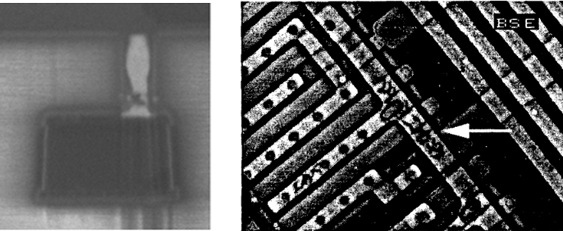
The figures above show electromigration and stress induced voids in the metallization under passivation. The stress induced voids occurred after the part was stored at 250C for 5000 hours.
Failure Analysis
– A failing to do or perform
– Examination of a thing to determine its parts or elements
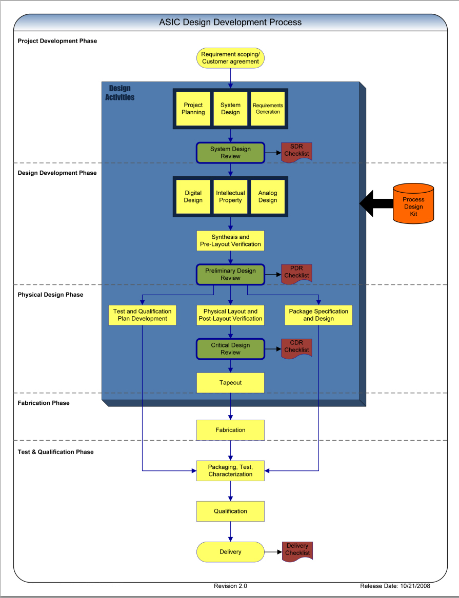
Failure Analysis is a diagnostic process for determining the root cause of failure.
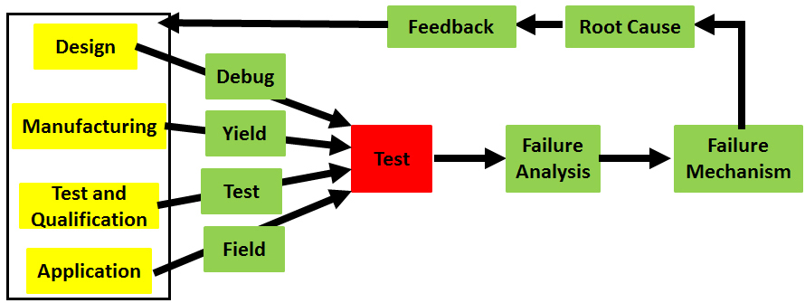
At Sandia, we have experts who invent, develop and utilize different tools and techniques for root cause failure analysis. Our expertise is in Silicon CMOS, III-V Compound Semiconductors, MEMS, Photovoltaics and Optoelectronics. We support our customers through the product life cycle. A basic FA process flow through the product life cycle is shown below:
Role of FA:
In product design and development, failure analysis assists with design debug to examine non-functioning or partially functioning devices. This effort requires close teaming with designers to expedite development times and bring the product to market more quickly.
Failure analysis of test structures & full product from yield failures during the semiconductor manufacturing process provides critical insight into manufacturing problems. Successful analysis and feedback leads to rapid yield ramping and improvements in the process flow. Requires close teaming with process engineers.
During qualification and reliability evaluation, failure analysis provides critical information on how the device failed during those operating conditions. Requires close teaming with product and reliability engineers.
Failure analysis of customer returns is critical to keeping consumer confidence in your product and company high. Failures are typically one of a kind requiring special handling so mistakes are not acceptable.
Failure Classification
Failures are classified as either hard, soft or intermittent fails.
Hard failures are those that are damaged or exhibit a significant loss of functionality.
• Shorts, opens and some semiconductor defects
Soft failures are failures that occur under certain environmental or operating conditions but not all operating conditions
• Temperature, voltage or frequency dependent failures
Intermittent failures occur under seemingly random conditions and are difficult to reproduce under the same operating conditions
Many tools and techniques used by Sandia for root cause failure analysis are listed below:
Failure analysis of semiconductor devices requires inspection and stimulation. Optical microscopy techniques are one tool used to visually inspect semiconductor devices at the system, sub-system, package, die or wafer level. Optical techniques such as bright field, dark field or Nomarski are used to provide information on structural anomalies, contamination and other features of a device.
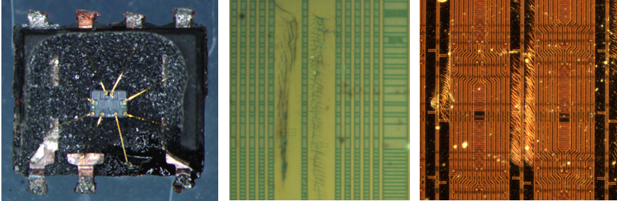
Bright field optical image of a depcapsulated IC exposing the die and wire bonds
Nomarski optical images of cracks in the passivation on the surface of an IC
Dark-field image
Laser based techniques are used to alter the electrical characteristics of a device, normally at a defect site. These techniques measure an electrical response of a device as a result of Illumination from an above or sub-band gap laser. Some techniques used for failure analysis include Optical Beam Induced Current (OBIC), Light-Induced Voltage Alteration (LIVA), Thermally-Induced Voltage Alteration (TIVA), Seebeck Effect Imaging (SEI) and Soft Defect Localization (SDL).
OBIC is similar to EBIC but is performed using a scanning optical microscope. The optical beam interacts with the space-charge region of a semiconductor device producing an electrical response.
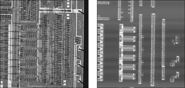
(left)Reflected light image of an IC (right)OBIC image of the same IC
LIVA uses above band-gap light sources to generate photocurrent that affects device operation. The generated photocurrent is used to alter electrical characteristics of a device and measure its electrical response. This technique can be applied from either the front or backside of the device.
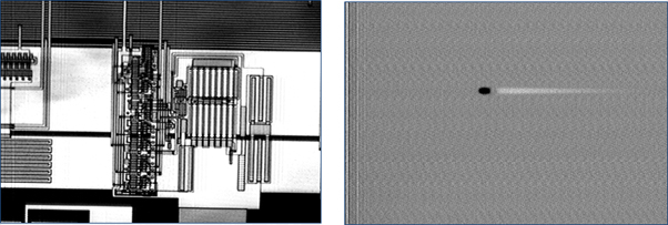
(left)Reflected light LIVA image of an IC (right)Backside LIVA image of a defect in the IC
Thermally-Induced Voltage Alteration is an FA technique that uses a sub-bandgap laser to produce localized heating in a device. The localized heating changes the resistance producing a change in the semiconductor device power demand. This this technique can be used through the front and back side of a device.
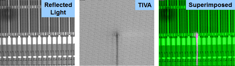
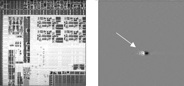
1340 nm light source scanned across an IC shows a signal in the middle of a circuit. The signal is the suspect failure site. When superimposed, the position of the failure site is mapped back to the reflected light image enabling defect localization for further analysis.
Thermal gradients produce voltage gradients on open interconnections. Localized heating changes voltage in open conductors and alters the power demands on the semiconductor device. Similar to TIVA and LIVA, the image of the changes in IC power demand are mapped with the laser position to localize the defect site.
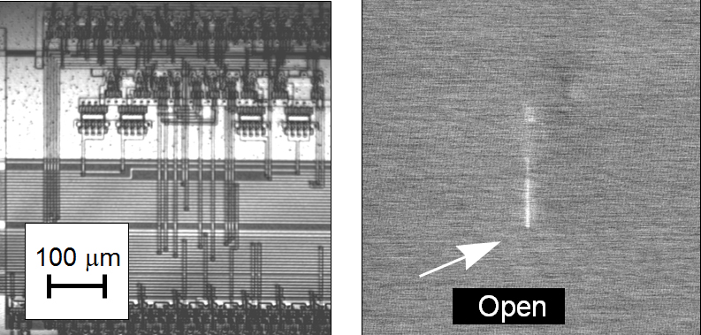
Reflected light and SEI image showing the location of an open in an IC
Soft Defect Localization is an analysis technique that uses localized heating to detect changes in pass/fail conditions. The changes in pass/fail conditions are used to produce image contrast identifying the suspect failure site.
Reflected light image with corresponding SDL image showing a region of the circuitry in a failed condition when the laser passes over it
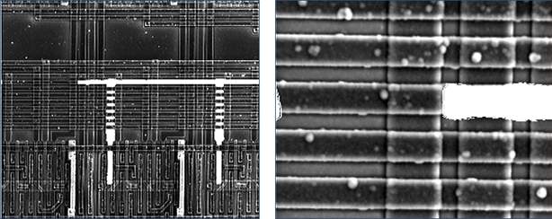
Light Emission (LE): failure analysis capability used to detect and localize photon emitting defects in semiconductor devices. Normal operating devices also produce light under certain conditions, defects such as hot carrier production, gate oxide shorts, saturated transistors, leaky junctions, latch-up, snap-back etc. can emit light. LE can be applied at wafer, package or board level.
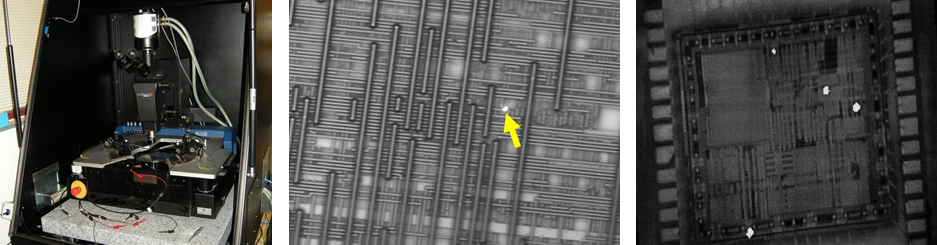
Light emission system mounted in a probe station for die, package or board level FA.
LE indicates general location of possibledefect. Scattering from upper metal layers prevents precise localization
High current in a microcontroller emitting light at multiple sites
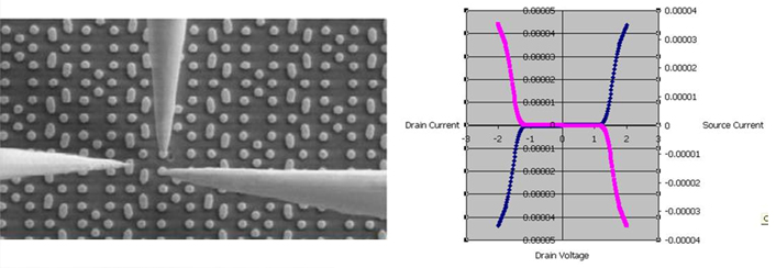
Electrical characterization techniques are employed to determine the electrical properties and/or behavior of a device to diagnose internal fault locations. Often used in failure validation/verification. External chip data such as scan-based diagnostics, fault dictionaries, schmoo plots, IDDQ versus pattern, timing, voltage, temp, and memory bit-fail maps are a few tools available for failure verification. Other less complicated techniques such as curve tracing, I-V and C-V profiling, 2 and 4 point probing can be used to determine resistivity, carrier concentration, mobility, contact resistance, depletion width and more.
At Sandia, many tools are used to electrically stimulate or measure the response of a semiconductor device for root cause failure analysis. Equipment such as parametric analyzers, waveform generators, curve tracers, automated test equipment, etc., have been used for root cause failure analysis.
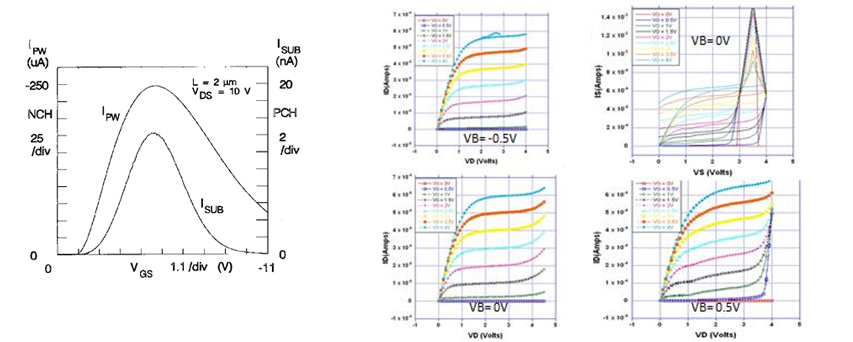
I-V curve showing n-channel MOSFET output is much larger than p-channel output
Electrical test data showing transistor I-V curves changing with applied bias
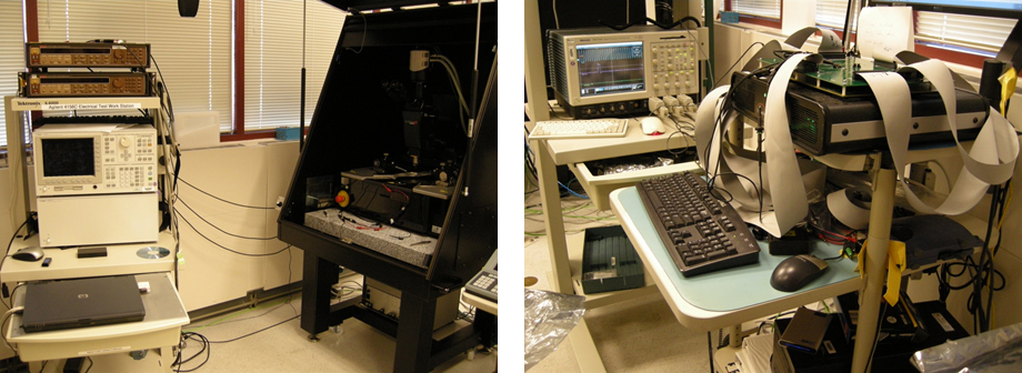
Power supplies and semiconductor parametric analyzer used to bias and measure the output from a probed device
Teseda test system with oscilloscope analyzing a device subjected to a subset of test vectors
Failure analysis techniques performed using a Scanning Electron Microscope (SEM), Transmission Electron Microscope (TEM) or Focused Ion Beam (FIB) use signals generated from an electron or ion beam source to produce an image. These signals such as secondary or backscattered electrons and characteristic x-rays are used to examine the structure or electrical activity of a device. Tools and techniques employed at Sandia include:
Scanning Electron Microscopy provides structural information using Secondary Electrons (SE) or Backscattered Electrons (BSE). SEs are electrons from the first few nanometers from the surface used to generate a topographic image. BSEs are used to detect contrast between areas with different chemical compositions.Sandia’s FA department uses an environmental SEM equipped with an Energy Dispersive X-Ray Spectrometer and a Nanoprobe system.
(left)SE image of a Vertical Cavity Surface Emitting Laser (VCSEL) detailing surface grain structure and material stack. Image taken in cross-section. (right)BSE image compared to SE image
Voltage Contrast provides a visual indication of voltage on device interconnections. In FA, VC is used to identify opens or shorts in electronic components.
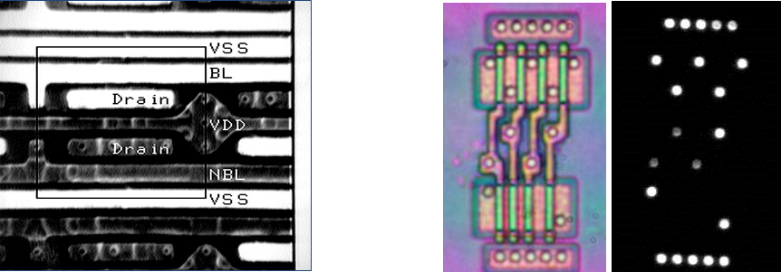
Voltage Contrast Image – VC on a deprocessed device shows active regions of a circuit with applied stimulus
Right: Floating Substrate Passive Voltage Contrast – Optical Image(L) and PVC Image(R)
Resistive Contrast Imaging is an FA technique using an electron beam to generate a relative Resistance map between two ore more test nodes on a device. A defect in a device will create an abrupt transition indicating a change in resistance
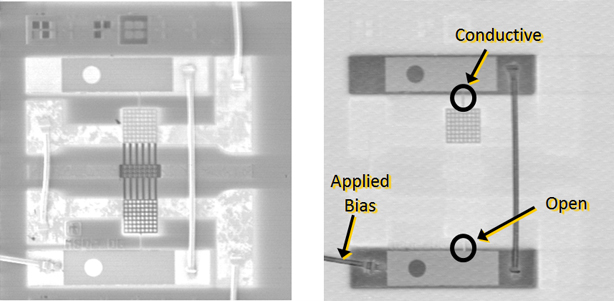
Secondary Electron Image
10 keV Resistive Contrast Image
RCI applied to an RF MEMS switch locates an open on a support beam. Applied bias shows contrast on the top pad (conductive) and no signal on the bottom pad (open).
Charge-Induced Voltage Alteration (CIVA) is an FA technique used to identify opens in microelectronic devices. The technique can be used at high and low energy levels and magnifications. Low Energy CIVA (LECIVA) reduces the irradiation damage to the IC under test.
CIVA/SE images taken at low (left) and high (right) magnifications revealing an open in an IC.
Electron Beam Induced Current is an analysis technique used to identify buried junctions or defects in semiconductor devices.
EBIC image of defects in a diode
Nanoprobing is an analysis technique used to measure electrical characteristics of individual circuits at very small dimensions.
Nanoprobing of a 65 nm transistor showing electrical properties at the source and drain
Transmission Electron Microscopy provides detailed structural information using a beam of electrons transmitted through an ultra-thin sample.
Plan-view TEM showing a dislocation network in the active region of a VCSEL
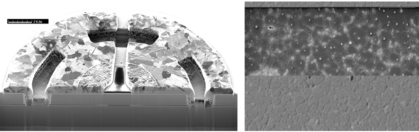
Focused Ion Beam (FIB): uses a liquid metal ion source to sputter material from a sample. Material is removed to perform local cross-sectional analysis providing key structural information at a defect or failure site. Material such as Platinum or Silicon Oxide can be deposited to create or modify electrical behavior of a device. Sandia’s FA group uses a dual-beam FIB system equipped with an Energy Dispersive X-ray Spectrometer (EDS) and various chemistries for material deposition and removal. Another FIB system also equipped with several chemistries is used for backside circuit edit.
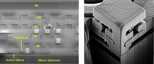
Cross-section of a device showing damage to M3 lines leading to a short failure
Cross-section of a MEMS pin joint showing wear and debris at contacting surfaces
Focused Ion Beam Circuit Edit: uses materials chemistry for deposition and removal of conductors and insulators to edit integrated circuits. Circuit edits can be performed from either the front or back side of the device.
Front side and deposition of probe padsenable device editing and electrical probing
Backside FIB trench to the device.
The Energy Dispersive X-ray Spectroscopy provides elemental information based on the emission of characteristic x-rays generated during electron beam/sample interaction. This technique can be used in either TEM, SEM or FIB platforms.
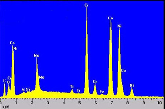
EDS Spectra taken from an alloy sample
Failure analysis techniques performed using a Infrared Thermography/Thermal Imaging or Lock-In Thermography use heat or thermal signals generated from a device during operation. Small leakage currents typically cause elevated temperature during operation of a device. A special camera is used to detect signals generated in the near-infrared to infrared range. Tools and techniques employed at Sandia include:
The Thermal Imaging System locates “hot spots” on a device during operation. This system has been used to identify locally heated areas for board-level and package level FA.
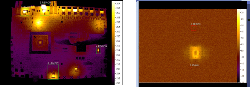
Board-level thermal imaging identifying multiple components heating up during operation
Package level thermal imaging showing a part heating up during operation
Lock-In Thermography provides spatially resolved detection of hot spots generated by leakage currents in electronic devices.
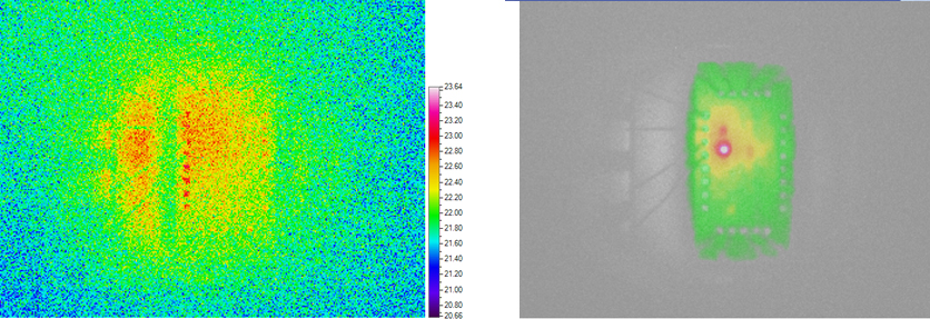
Thermal Image (DC Operation)- Thermal image showing a large hot spot spanning most of the package
Lock-In Thermograph (Pulsed DC) – Lock-in thermograph of the same package under pulsed DC operation localizes the region generating heat (current leakage site)
Deprocessing
Many failure analysis techniques require direct access to the device or deprocessing for defect localization. At Sandia, we use a variety of techniques to gain access to a device. Some deprocessing capabilities used in FA include:
- Sawing – for component removal from boards, etc.
- Polishing
- Jet etching – locally removing plastic from a package while keeping the device functional
- Chemical etching
- Staining – use of acids and bases to delineate defects in materials
Polishing tool used for package and die level deprocessing
Jet etch tool for plastic package decapsulation
Decapsulated package exposing the die
Fact Sheets, Publications, References, Animations, Licensing IP Opportunities
Failure Analysis Publications and Patents
J. Beutler, J. Clement, M. Miller, J. Stevens, E.I. Cole Jr., “Visible Alight LVP on Ultra-Thinned Substratesâ€, 40th International Symposium for Testing and Failure Analysis, pp. 110-114
M. A. Miller, E. I. Cole Jr., P. Tangyunyong, “Characterization of Green and Ultraviolet LEDs by Laser-based FA Techniquesâ€, 36th International Symposium for Testing and Failure Analysis, pp. 275-280
E.I. Cole Jr., “Beam Based Defect Localizationâ€, Electronic Device Failure Analysis Desk Reference 5th Ed., pp. 406-416
J.A. Walraven, I. De Wolf, B. Waterson, “Failure Analysis of Microelectromechanical Systemsâ€, Electronic Device Failure Analysis Desk Reference 5th Ed., pp. 193-218
M.W. Jenkins, P. Tangyunyong, E.I. Cole Jr., J. M. Soden, J.A. Walraven, A. A. Pimentel, “Floating Substrate Passive Voltage Contrast (FSPVC)â€, 32nd International Symposium for Testing and Failure Analysis, pp. 321-327
M.R. Bruce, V.J. Bruce, D.H. Eppes, J. Wilcox, E.I. Cole Jr., P. Tangyunyong, C.F. Hawkins, “Soft Defect Localization (SDL) on ICs, 28th 32nd International Symposium for Testing and Failure Analysis, pp. 21-27
System and Method for Floating-Substrate Passive Voltage Contrast, Patent # 6546513
Thermally-Induced Voltage Alteration for Analysis of Microelectromechanical Systems, Patent # 6407560
Localization of resistive Interconnections on Integrated Circuits, Patent # 7062399
Apparatus and Method for Analyzing Functional Failures in Integrated Circuits, Patent # 6031386
Thermally-Induced Voltage Alteration for Integrated Circuit Analysis, Patent # 60781853 .
Capacitive Charge Generation Apparatus and Method for Testing Circuits, Patent # 5781017
Integrated Circuit Failure Analysis by Low-energy Charge Induced Voltage Alteration, Patent # 5523694.
Magnetic Force Microscopy (MFM) Techniques for Internal Current Probing of Integrated Circuits, Patent # 5465046
Light-Induced Voltage3 Alteration for Integrated Circuit Analysis, Patent # 5430305