| Plasma-based method for delayering of circuits |
US12532680B2 |
01/20/2026
|
| Plasma-based method for delayering of circuits |
US12532680B2 |
01/20/2026
|
| Area selective deposition templated by hydrogen and halogen resists |
US12518967B1 |
01/06/2026
|
| Area selective deposition templated by hydrogen and halogen resists |
US12518967B1 |
01/06/2026
|
| Single clock delay step in multi-stage switched-capacitor delays |
US12489434B1 |
12/02/2025
|
| Single clock delay step in multi-stage switched-capacitor delays |
US12489434B1 |
12/02/2025
|
| Large programmable delay at high frequency through aliasing |
US12476624B1 |
11/18/2025
|
| Large programmable delay at high frequency through aliasing |
US12476624B1 |
11/18/2025
|
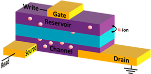
| Electrochemical random access memory device with contact layer as a heat source |
US12446479B1 |
10/14/2025
|
| Electrochemical random access memory device with contact layer as a heat source |
US12446479B1 |
10/14/2025
|
| Electrochemical random access memory device with contact layer as a heat source |
US12446479B1 |
10/14/2025
|
| Complementary current reuse even harmonic frequency multiplier |
US12438506B1 |
10/07/2025
|
| Integrated photonics with active polarization control |
US12429716B1 |
09/30/2025
|
| Integrated photonics with active polarization control |
US12429716B1 |
09/30/2025
|
| Low power mixed gas sensor |
US12422421B2 |
09/23/2025
|
| Low power mixed gas sensor |
US12422421B2 |
09/23/2025
|
| Ultraviolet and visible light integrated acousto-optic modulators |
US12416824B1 |
09/16/2025
|
| Continuously variable optical confinement for optical amplifiers |
US12355209B1 |
07/08/2025
|
| Meissner-effect transition-edge-sensor microcalorimeter |
US12352634B1 |
07/08/2025
|
| Meissner-effect transition-edge-sensor microcalorimeter |
US12352634B1 |
07/08/2025
|
| Continuously variable optical confinement for optical amplifiers |
US12355209B1 |
07/08/2025
|
| Transistor with curvilinear gate configuration for improved thermal distribution |
US12310082B1 |
05/20/2025
|
| Method for modifying or verifying a circuit by inserting a saboteur circuit |
US12210427B1 |
01/28/2025
|
| Method for modifying or verifying a circuit by inserting a saboteur circuit |
US12210427B1 |
01/28/2025
|
| Acoustoelectric optomechanical devices |
US12204183B1 |
01/21/2025
|
| Acoustoelectric optomechanical devices |
US12204183B1 |
01/21/2025
|
| Interlocking proof mass for mems inertial sensing device |
US12129167B1 |
10/29/2024
|
| Interlocking proof mass for mems inertial sensing device |
US12129167B1 |
10/29/2024
|
| Miniature ultra-low-power LNA employing current reuse and bias sharing |
US12095424B1 |
09/17/2024
|
| Self-insulating metal vias in magnetic micro-devices |
US12094629B1 |
09/17/2024
|
| Self-insulating metal vias in magnetic micro-devices |
US12094629B1 |
09/17/2024
|
| Miniature ultra-low-power LNA employing current reuse and bias sharing |
US12095424B1 |
09/17/2024
|
| Heterogeneous radiation-hardened computing system |
US12079159B1 |
09/03/2024
|
| Heterogeneous radiation-hardened computing system |
US12079159B1 |
09/03/2024
|
| Multichannel transistor with improved gate conformation |
US12068216B1 |
08/20/2024
|
| CMOS compatible low-resistivity Al—Sc metal etch stop |
US12034050B1 |
07/09/2024
|
| CMOS compatible low-resistivity Al—Sc metal etch stop |
US12034050B1 |
07/09/2024
|
| Systems and methods for resolving a number of incident RF-range photons |
US12029141B1 |
07/02/2024
|
| Systems and methods for resolving a number of incident RF-range photons |
US12029141B1 |
07/02/2024
|
| Systems and methods for resolving a number of incident RF-range photons |
US12029141B1 |
07/02/2024
|
| Heterogeneously integrated acoustoelectric amplifiers |
US11948979B1 |
04/02/2024
|
| Heterogeneously integrated acoustoelectric amplifiers |
US11948979B1 |
04/02/2024
|
| Thermally sensitive state change ionic redox transistor |
US11942282B1 |
03/26/2024
|
| Monolithic integration of optical waveguides with metal routing layers |
US11906351B1 |
02/20/2024
|
| Monolithic integration of optical waveguides with metal routing layers |
US11906351B1 |
02/20/2024
|
| Systems, methods and computer program products for charging autonomous wireless sensors in subsurface environments |
US11876398B1 |
01/16/2024
|
| High aspect ratio gratings fabricated by electrodeposition |
US11798844B1 |
10/24/2023
|
| Method of chemical doping that uses CMOS-compatible processes |
US11798808B1 |
10/24/2023
|
| Concentrated thermal tuner for optical microdisk devices |
US11796841B1 |
10/24/2023
|
| High aspect ratio gratings fabricated by electrodeposition |
US11798844B1 |
10/24/2023
|
| Method of chemical doping that uses CMOS-compatible processes |
US11798808B1 |
10/24/2023
|
| Multi-chip photonics transceiver |
US11726276B1 |
08/15/2023
|
| Multi-chip photonics transceiver |
US11726276B1 |
08/15/2023
|
| MEMS-tunable optical ring resonator |
US11722120B1 |
08/08/2023
|
| MEMS-tunable optical ring resonator |
US11722120B1 |
08/08/2023
|
| Heterogeneous integration of an electro-optical platform |
US11675126B1 |
06/13/2023
|
| Heterogeneous integration of an electro-optical platform |
US11675126B1 |
06/13/2023
|
| Integrated silicon optical amplifier with reduced residual pump |
US11652330B1 |
05/16/2023
|
| Integrated silicon optical amplifier with reduced residual pump |
US11652330B1 |
05/16/2023
|
| Low power sensor for NOx detection |
US11573217B2 |
02/07/2023
|
| Low power sensor for NOx detection |
US11573217B2 |
02/07/2023
|
| Piezoelectric deformable photonic devices |
US11569431B1 |
01/31/2023
|
| Piezoelectric deformable photonic devices |
US11569431B1 |
01/31/2023
|
| Miniaturized vacuum package and methods of making same |
US11551921B1 |
01/10/2023
|
| Enhanced microfabrication using electrochemical techniques |
US11549903B1 |
01/10/2023
|
| Miniaturized vacuum package and methods of making same |
US11551921B1 |
01/10/2023
|
| Enhanced microfabrication using electrochemical techniques |
US11549903B1 |
01/10/2023
|
| Compact laser source with frequency modulators generating multiple lines |
US11545815B1 |
01/03/2023
|
| Compact laser source with frequency modulators generating multiple lines |
US11545815B1 |
01/03/2023
|
| Analog vector-matrix multiplication by capacitive elements with resistive state storage |
US11494464B1 |
11/08/2022
|
| Analog vector-matrix multiplication by capacitive elements with resistive state storage |
US11494464B1 |
11/08/2022
|
| Metal stack templates for suppressing secondary grains in sca1n |
US11482660B1 |
10/25/2022
|
| Metal stack templates for suppressing secondary grains in sca1n |
US11482660B1 |
10/25/2022
|
| Thermally sensitive ionic redox transistor |
US11450802B1 |
09/20/2022
|
| Thermally sensitive ionic redox transistor |
US11450802B1 |
09/20/2022
|
| Photolithography of atomic layer resist |
US11424135B1 |
08/23/2022
|
| Photolithography of atomic layer resist |
US11424135B1 |
08/23/2022
|
| Phase-wrapping method for beam steering in optical phased arrays |
US11409183B1 |
08/09/2022
|
| Phase-wrapping method for beam steering in optical phased arrays |
US11409183B1 |
08/09/2022
|
| Hybrid piezoelectric microresonator |
US11387802B1 |
07/12/2022
|
| Tunneling full-wave infrared rectenna |
US11296240B1 |
04/05/2022
|
| Tunneling full-wave infrared rectenna |
US11296240B1 |
04/05/2022
|
| Active shunt capacitance cancelling oscillator for resonators |
US11171604B1 |
11/09/2021
|
| Active shunt capacitance cancelling oscillator for resonators |
US11171604B1 |
11/09/2021
|
| Optical coupler for heterogeneous integration |
US11163115B1 |
11/02/2021
|
| Optical coupler for heterogeneous integration |
US11163115B1 |
11/02/2021
|
| Trapped ion platform with optical input and output |
US11150609B1 |
10/19/2021
|
| Trapped ion platform with optical input and output |
US11150609B1 |
10/19/2021
|
| Apparatus and method to measure semiconductor optical absorption using microwave charge sensing |
US11125700B2 |
09/21/2021
|
| Apparatus and method to measure semiconductor optical absorption using microwave charge sensing |
US11125700B2 |
09/21/2021
|
| Microfabricated ion trap chip with in situ radio-frequency sensing |
US11056332B1 |
07/06/2021
|
| Microfabricated ion trap chip with in situ radio-frequency sensing |
US11056332B1 |
07/06/2021
|
| Optical devices enabled by vertical dielectric Mie resonators |
US11017186B2 |
05/25/2021
|
| Microfabricated ion trap chip with an integrated microwave antenna |
US10984976B1 |
04/20/2021
|
| Dual frequency transceiver device |
US10984300B2 |
04/20/2021
|
| Dual frequency transceiver device |
US10984300B2 |
04/20/2021
|
| Microfabricated ion trap chip with an integrated microwave antenna |
US10984976B1 |
04/20/2021
|
| Focusing transformers/filters in isotropic/anisotropic piezoelectrics |
US10979018B1 |
04/13/2021
|
| Method of fabricating photosensitive devices with reduced process-temperature budget |
US10910508B1 |
02/02/2021
|
| Method of fabricating photosensitive devices with reduced process-temperature budget |
US10910508B1 |
02/02/2021
|
| Heterogeneously integrated electro-optic modulator |
US10788689B1 |
09/29/2020
|
| Heterogeneously integrated electro-optic modulator |
US10788689B1 |
09/29/2020
|
| Heterogeneously integrated electro-optic modulator |
US10788689B1 |
09/29/2020
|
| Hybrid semiconductor-piezoacoustic radiofrequency device |
US10666222B1 |
05/26/2020
|
| ScAIN etch mask for highly selective etching |
US10651048B1 |
05/12/2020
|
| ScAIN etch mask for highly selective etching |
US10651048B1 |
05/12/2020
|
| Active mechanical-environmental-thermal MEMS device for nanoscale characterization |
US10641733B2 |
05/05/2020
|
| Active mechanical-environmental-thermal MEMS device for nanoscale characterization |
US10641733B2 |
05/05/2020
|
| Fabrication of multilayered carbon MEMS devices |
US10570010B1 |
02/25/2020
|
| Fabrication of multilayered carbon MEMS devices |
US10570010B1 |
02/25/2020
|
| Supply-noise-rejecting current source |
US10566936B1 |
02/18/2020
|
| Supply-noise-rejecting current source |
US10566936B1 |
02/18/2020
|
| Regrowth method for fabricating wide-bandgap transistors, and devices made thereby |
US10553697B1 |
02/04/2020
|
| Regrowth method for fabricating wide-bandgap transistors, and devices made thereby |
US10553697B1 |
02/04/2020
|
| Thallium bromide (TIBr) semiconductors and devices with extended life apparatus, methods, and system |
US10516068B1 |
12/24/2019
|
| Thallium bromide (TIBr) semiconductors and devices with extended life apparatus, methods, and system |
US10516068B1 |
12/24/2019
|
| Evanescently coupled piezoelectric acoustic devices |
US10491190B1 |
11/26/2019
|
| Non-inverting multi-mode oscillator |
US10483912B1 |
11/19/2019
|
| Low-power MEMS wakeup system |
US10481672B1 |
11/19/2019
|
| Low-power MEMS wakeup system |
US10481672B1 |
11/19/2019
|
| Non-inverting multi-mode oscillator |
US10483912B1 |
11/19/2019
|
| Systems and methods for interferometric end point detection for a focused ion beam fabrication tool |
US10446369B1 |
10/15/2019
|
| Systems and methods for interferometric end point detection for a focused ion beam fabrication tool |
US10446369B1 |
10/15/2019
|
| Coupled memristor devices to enable feedback control and sensing of micro/nanoelectromechanical actuator and sensors |
US10392243B2 |
08/27/2019
|
| Coupled memristor devices to enable feedback control and sensing of micro/nanoelectromechanical actuator and sensors |
US10392243B2 |
08/27/2019
|
| Regrowth method for fabricating wide-bandgap transistors, and devices made thereby |
US10388753B1 |
08/20/2019
|
| Regrowth method for fabricating wide-bandgap transistors, and devices made thereby |
US10388753B1 |
08/20/2019
|
| Bus based timed input output module |
US10289573B1 |
05/14/2019
|
| Bus based timed input output module |
US10289573B1 |
05/14/2019
|
| Variable bandwidth filter |
US10267896B1 |
04/23/2019
|
| Variable bandwidth filter |
US10267896B1 |
04/23/2019
|
| Communication device and method of making the same |
US10235614B1 |
03/19/2019
|
| Communication device and method of making the same |
US10235614B1 |
03/19/2019
|
| Via configuration for wafer-to-wafer interconnection |
US10224312B1 |
03/05/2019
|
| Via configuration for wafer-to-wafer interconnection |
US10224312B1 |
03/05/2019
|
| Method for simultaneous modification of multiple semiconductor device features |
US10217704B1 |
02/26/2019
|
| Hybrid CMOS-MEMS devices adapted for high-temperature operation and method for their manufacture |
US10214415B1 |
02/26/2019
|
| Hybrid CMOS-MEMS devices adapted for high-temperature operation and method for their manufacture |
US10214415B1 |
02/26/2019
|
| Hybrid CMOS-MEMS devices adapted for high-temperature operation and method for their manufacture |
US10214415B1 |
02/26/2019
|
| Gm-C filter and multi-phase clock circuit |
US10181840B1 |
01/15/2019
|
| Gm-C filter and multi-phase clock circuit |
US10181840B1 |
01/15/2019
|
| Passive radiative cooling of a body |
US10173792B1 |
01/08/2019
|
| Passive radiative cooling of a body |
US10173792B1 |
01/08/2019
|
| Trimming method for microresonators and microresonators made thereby |
US10148244B1 |
12/04/2018
|
| Trimming method for microresonators and microresonators made thereby |
US10148244B1 |
12/04/2018
|
| Microsystems-based method and apparatus for passive detection and processing of radio-frequency signals |
US10141495B1 |
11/27/2018
|
| Vertically integrated optoelectronics package for MEMS devices |
US10139564B1 |
11/27/2018
|
| Vertically integrated optoelectronics package for MEMS devices |
US10139564B1 |
11/27/2018
|
| Microsystems-based method and apparatus for passive detection and processing of radio-frequency signals |
US10141495B1 |
11/27/2018
|
| Graphene heat dissipating structure |
US10096536B1 |
10/09/2018
|
| Graphene heat dissipating structure |
US10096536B1 |
10/09/2018
|
| Supply-noise-rejecting current source |
US10090826B1 |
10/02/2018
|
| System on chip module configured for event-driven architecture |
US10089160B2 |
10/02/2018
|
| System on chip module configured for event-driven architecture |
US10089160B2 |
10/02/2018
|
| Supply-noise-rejecting current source |
US10090826B1 |
10/02/2018
|
| Systems and methods to maintain optimum stoichiometry for reactively sputtered films |
US10074522B1 |
09/11/2018
|
| Method and apparatus of enhanced thermoelectric cooling and power conversion |
US10072879B1 |
09/11/2018
|
| Method and apparatus of enhanced thermoelectric cooling and power conversion |
US10072879B1 |
09/11/2018
|
| Optomechanical force sensors, cantilevers, and systems thereof |
US10031158B1 |
07/24/2018
|
| Optomechanical force sensors, cantilevers, and systems thereof |
US10031158B1 |
07/24/2018
|
| Methods for suppressing spurious modes in microresonators |
US10009002B1 |
06/26/2018
|
| Flexible packaging for microelectronic devices |
US9978895B2 |
05/22/2018
|
| Flexible packaging for microelectronic devices |
US9978895B2 |
05/22/2018
|
| Packaging system with cleaning channel and method of making the same |
US9972553B1 |
05/15/2018
|
| Packaging system with cleaning channel and method of making the same |
US9972553B1 |
05/15/2018
|
| Attenuation of spurious responses in electromechanical filters |
US9941857B1 |
04/10/2018
|
| Attenuation of spurious responses in electromechanical filters |
US9941857B1 |
04/10/2018
|
| Superlattice photodetector having improved carrier mobility |
US9929293B1 |
03/27/2018
|
| Superlattice photodetector having improved carrier mobility |
US9929293B1 |
03/27/2018
|
| Diode and method of making the same |
US9917149B1 |
03/13/2018
|
| Gallium beam lithography for superconductive structure formation |
US9882113B1 |
01/30/2018
|
| Gallium beam lithography for superconductive structure formation |
US9882113B1 |
01/30/2018
|
| Second harmonic generation in resonant optical structures |
US9865987B1 |
01/09/2018
|
| Second harmonic generation in resonant optical structures |
US9865987B1 |
01/09/2018
|
| Ion-barrier for memristors/ReRAM and methods thereof |
US9831427B1 |
11/28/2017
|
| Method of making thermally-isolated silicon-based integrated circuits |
US9824932B1 |
11/21/2017
|
| Electroabsorption optical modulator |
US9823497B1 |
11/21/2017
|
| Electroabsorption optical modulator |
US9823497B1 |
11/21/2017
|
| Method of making thermally-isolated silicon-based integrated circuits |
US9824932B1 |
11/21/2017
|
| System on chip module configured for event-driven architecture |
US9792250B1 |
10/17/2017
|
| Processing device with self-scrubbing logic |
US9792184B2 |
10/17/2017
|
| System on chip module configured for event-driven architecture |
US9792250B1 |
10/17/2017
|
| Processing device with self-scrubbing logic |
US9792184B2 |
10/17/2017
|
| Apparatus for assembly of microelectronic devices |
US9763370B2 |
09/12/2017
|
| Apparatus for assembly of microelectronic devices |
US9763370B2 |
09/12/2017
|
| Graphene heat dissipating structure |
US9721867B1 |
08/01/2017
|
| Graphene heat dissipating structure |
US9721867B1 |
08/01/2017
|
| Fast frequency divider circuit using combinational logic |
US9667231B1 |
05/30/2017
|
| Method of making a silicon nanowire device |
US9660026B1 |
05/23/2017
|
| Wafer scale oblique angle plasma etching |
US9659797B1 |
05/23/2017
|
| Method of making a silicon nanowire device |
US9660026B1 |
05/23/2017
|
| Wafer scale oblique angle plasma etching |
US9659797B1 |
05/23/2017
|
| Thermally-isolated silicon-based integrated circuits and related methods |
US9646874B1 |
05/09/2017
|
| Thermally-isolated silicon-based integrated circuits and related methods |
US9646874B1 |
05/09/2017
|
| Single crystal micromechanical resonator |
US9641154B2 |
05/02/2017
|
| Single crystal micromechanical resonator |
US9641154B2 |
05/02/2017
|
| Plasmon-assisted optical vias for photonic ASICS |
US9599781B1 |
03/21/2017
|
| Visible light laser voltage probing on thinned substrates |
US9599667B1 |
03/21/2017
|
| Plasmon-assisted optical vias for photonic ASICS |
US9599781B1 |
03/21/2017
|
| Visible light laser voltage probing on thinned substrates |
US9599667B1 |
03/21/2017
|
| Photoelectrochemically driven self-assembly method |
US9548411B2 |
01/17/2017
|
| Methods of depositing an alpha-silicon-carbide-containing film at low temperature |
US9546420B1 |
01/17/2017
|
| Photoelectrochemically driven self-assembly method |
US9548411B2 |
01/17/2017
|
| Methods of depositing an alpha-silicon-carbide-containing film at low temperature |
US9546420B1 |
01/17/2017
|
| Silicon nanowire device and method for its manufacture |
US9536947B1 |
01/03/2017
|
| Silicon nanowire device and method for its manufacture |
US9536947B1 |
01/03/2017
|
| Single crystal micromechanical resonator and fabrication methods thereof |
US9525398B1 |
12/20/2016
|
| Single crystal micromechanical resonator and fabrication methods thereof |
US9525398B1 |
12/20/2016
|
| Transparent contacts for stacked compound photovoltaic cells |
US9508881B2 |
11/29/2016
|
| Transparent contacts for stacked compound photovoltaic cells |
US9508881B2 |
11/29/2016
|
| Methods for dry etching semiconductor devices |
US9484216B1 |
11/01/2016
|
| Methods for dry etching semiconductor devices |
US9484216B1 |
11/01/2016
|
| Guided-wave photodiode using through-absorber quantum-well-intermixing and methods thereof |
US9477040B1 |
10/25/2016
|
| Guided-wave photodiode using through-absorber quantum-well-intermixing and methods thereof |
US9477040B1 |
10/25/2016
|
| Zero-power receiver |
US9460321B1 |
10/04/2016
|
| Silicon force sensor and method of using the same |
US9459161B1 |
10/04/2016
|
| Zero-power receiver |
US9460321B1 |
10/04/2016
|
| Silicon force sensor and method of using the same |
US9459161B1 |
10/04/2016
|
| Fabrication method for small-scale structures with non-planar features |
US9448336B1 |
09/20/2016
|
| Fabrication method for small-scale structures with non-planar features |
US9448336B1 |
09/20/2016
|
| Integrated field emission array for ion desorption |
US9425019B1 |
08/23/2016
|
| Multilevel resistive information storage and retrieval |
US9412446B1 |
08/09/2016
|
| Silicon force sensor |
US9383270B1 |
07/05/2016
|
| Silicon force sensor |
US9383270B1 |
07/05/2016
|
| Microresonator electrode design |
US9337800B1 |
05/10/2016
|
| Methods for resistive switching of memristors |
US9336870B1 |
05/10/2016
|
| Integrated circuit test-port architecture and method and apparatus of test-port generation |
US9311444B1 |
04/12/2016
|
| Integrated circuit test-port architecture and method and apparatus of test-port generation |
US9311444B1 |
04/12/2016
|
| Programmable electroacoustic filter apparatus and method for its manufacture |
US9276557B1 |
03/01/2016
|
| Processing device with self-scrubbing logic |
US9274895B1 |
03/01/2016
|
| Programmable electroacoustic filter apparatus and method for its manufacture |
US9276557B1 |
03/01/2016
|
| Processing device with self-scrubbing logic |
US9274895B1 |
03/01/2016
|
| Apparatuses and methods for tuning center frequencies |
US9270281B1 |
02/23/2016
|
| Apparatuses and methods for tuning center frequencies |
US9270281B1 |
02/23/2016
|
| Tuning method for microresonators and microresonators made thereby |
US9203134B1 |
12/01/2015
|
| Fully integrated and encapsulated micro-fabricated vacuum diode and method of manufacturing same |
US9202657B1 |
12/01/2015
|
| Tuning method for microresonators and microresonators made thereby |
US9203134B1 |
12/01/2015
|
| Fabrication of small-scale structures with non-planar features |
US9190736B1 |
11/17/2015
|
| Three-dimensional stacked structured ASIC devices and methods of fabrication thereof |
US9190392B1 |
11/17/2015
|
| Fabrication of small-scale structures with non-planar features |
US9190736B1 |
11/17/2015
|
| Three-dimensional stacked structured ASIC devices and methods of fabrication thereof |
US9190392B1 |
11/17/2015
|
| Separating semiconductor devices from substrate by etching graded composition release layer disposed between semiconductor devices and substrate including forming protuberances that reduce stiction |
US9029239B2 |
05/12/2015
|
| Separating semiconductor devices from substrate by etching graded composition release layer disposed between semiconductor devices and substrate including forming protuberances that reduce stiction |
US9029239B2 |
05/12/2015
|
| Protecting integrated circuits from excessive charge accumulation during plasma cleaning of multichip modules |
US9013046B1 |
04/21/2015
|
| Protecting integrated circuits from excessive charge accumulation during plasma cleaning of multichip modules |
US9013046B1 |
04/21/2015
|
| Membrane projection lithography |
US8981337B1 |
03/17/2015
|
| Membrane projection lithography |
US8981337B1 |
03/17/2015
|
| Processes for multi-layer devices utilizing layer transfer |
US8946052B2 |
02/03/2015
|
| Processes for multi-layer devices utilizing layer transfer |
US8946052B2 |
02/03/2015
|
| Method of forming through substrate vias (TSVs) and singulating and releasing die having the TSVs from a mechanical support substrate |
US8906803B2 |
12/09/2014
|
| Method of forming through substrate vias (TSVs) and singulating and releasing die having the TSVs from a mechanical support substrate |
US8906803B2 |
12/09/2014
|
| Frequency selective infrared sensors |
US8897609B1 |
11/25/2014
|
| Structured wafer for device processing |
US8895364B1 |
11/25/2014
|
| Structured wafer for device processing |
US8895364B1 |
11/25/2014
|
| Frequency selective infrared sensors |
US8897609B1 |
11/25/2014
|
| Memristor using a transition metal nitride insulator |
US8872246B1 |
10/28/2014
|
| Method of manufacturing a fully integrated and encapsulated micro-fabricated vacuum diode |
US8814622B1 |
08/26/2014
|
| Micromachined force-balance feedback accelerometer with optical displacement detection |
US8783106B1 |
07/22/2014
|
| Plasmon absorption modulator systems and methods |
US8780431B1 |
07/15/2014
|
| Plasmon absorption modulator systems and methods |
US8780431B1 |
07/15/2014
|
| Infrared nanoantenna apparatus and method for the manufacture thereof |
US8750653B1 |
06/10/2014
|
| Full tape thickness feature conductors for EMI structures |
US8747591B1 |
06/10/2014
|
| Full tape thickness feature conductors for EMI structures |
US8747591B1 |
06/10/2014
|
| Infrared nanoantenna apparatus and method for the manufacture thereof |
US8750653B1 |
06/10/2014
|
| Parallel optical sampler |
US8730562B1 |
05/20/2014
|
| Structured wafer for device processing |
US8729673B1 |
05/20/2014
|
| Optically transduced MEMS gyro device |
US8726730B1 |
05/20/2014
|
| Structured wafer for device processing |
US8729673B1 |
05/20/2014
|
| Optically transduced MEMS gyro device |
US8726730B1 |
05/20/2014
|
| Optical domain analog to digital conversion methods and apparatus |
US8725004B1 |
05/13/2014
|
| Microscale autonomous sensor and communications module |
US8680810B1 |
03/25/2014
|
| Microscale autonomous sensor and communications module |
US8680810B1 |
03/25/2014
|
| Ovenized microelectromechanical system (MEMS) resonator |
US8669823B1 |
03/11/2014
|
| Die singulation method |
US8623744B1 |
01/07/2014
|
| Die singulation method |
US8623744B1 |
01/07/2014
|
| Micro electro mechanical system optical switching |
US8611706B1 |
12/17/2013
|
| MEMS packaging with etching and thinning of lid wafer to form lids and expose device wafer bond pads |
US8597985B1 |
12/03/2013
|
| MEMS packaging with etching and thinning of lid wafer to form lids and expose device wafer bond pads |
US8597985B1 |
12/03/2013
|
| Optical XOR gate |
US8582931B1 |
11/12/2013
|
| Optical XOR gate |
US8582931B1 |
11/12/2013
|
| Wafer-level packaging with compression-controlled seal ring bonding |
US8575748B1 |
11/05/2013
|
| Wafer-level packaging with compression-controlled seal ring bonding |
US8575748B1 |
11/05/2013
|
| Integrated field emission array for ion desorption |
US8536564B1 |
09/17/2013
|
| Lateral acoustic wave resonator comprising a suspended membrane of low damping resonator material |
US8525619B1 |
09/03/2013
|
| Microelectromechanical filter formed from parallel-connected lattice networks of contour-mode resonators |
US8497747B1 |
07/30/2013
|
| Die singulation method |
US8461023B1 |
06/11/2013
|
| Die singulation method |
US8461023B1 |
06/11/2013
|
| Frequency selective infrared sensors |
US8452134B1 |
05/28/2013
|
| Frequency selective infrared sensors |
US8452134B1 |
05/28/2013
|
| Microfabricated particle focusing device |
US8425749B1 |
04/23/2013
|
| Optical set-reset latch |
US8363990B1 |
01/29/2013
|
| Die singulation method and package formed thereby |
US8236611B1 |
08/07/2012
|
| Die singulation method and package formed thereby |
US8236611B1 |
08/07/2012
|
| Microelectromechanical (MEM) thermal actuator |
US8232858B1 |
07/31/2012
|
| Microelectromechanical (MEM) thermal actuator |
US8232858B1 |
07/31/2012
|
| Microelectromechanical inertial sensor |
US8205497B1 |
06/26/2012
|
| Microelectromechanical inertial sensor |
US8205497B1 |
06/26/2012
|
| Optical NOR gate |
US8014639B1 |
09/06/2011
|
| Optical NOR gate |
US8014639B1 |
09/06/2011
|
| Tunable surface plasmon devices |
US8009356B1 |
08/30/2011
|
| Tunable surface plasmon devices |
US8009356B1 |
08/30/2011
|
| Optical NAND gate |
US7995877B1 |
08/09/2011
|
| Optical NAND gate |
US7995877B1 |
08/09/2011
|
| Microelectromechanical pump utilizing porous silicon |
US7980828B1 |
07/19/2011
|
| Microfabricated ion frequency standard |
US7859350B1 |
12/28/2010
|
| Microfabricated ion frequency standard |
US7859350B1 |
12/28/2010
|
| Microfabricated bulk wave acoustic bandgap device |
US7836566B1 |
11/23/2010
|
| Microfabricated bulk wave acoustic bandgap device |
US7836566B1 |
11/23/2010
|
| Dual-range linearized transimpedance amplifier system |
US7825735B1 |
11/02/2010
|
| Dual-range linearized transimpedance amplifier system |
US7825735B1 |
11/02/2010
|
| Fabrication of thermal microphotonic sensors and sensor arrays |
US7820970B1 |
10/26/2010
|
| Optical data latch |
US7787719B1 |
08/31/2010
|
| Microfabricated bulk wave acoustic bandgap device |
US7733198B1 |
06/08/2010
|
| Microfabricated bulk wave acoustic bandgap device |
US7733198B1 |
06/08/2010
|
| Method for forming precision clockplate with pivot pins |
US7728248B1 |
06/01/2010
|
| Method for forming precision clockplate with pivot pins |
US7728248B1 |
06/01/2010
|
| Nanoeletromechanical switch and logic circuits formed therefrom |
US7719318B1 |
05/18/2010
|
| Microelectromechanical tunable inductor |
US7710232B1 |
05/04/2010
|
| Eddy-current-damped microelectromechanical switch |
US7633362B1 |
12/15/2009
|
| Microelectromechanical resonator and method for fabrication |
US7616077B1 |
11/10/2009
|
| Redox buffered hydrofluoric acid etchant for the reduction of galvanic attack during release etching of MEMS devices having noble material films |
US7597819B1 |
10/06/2009
|
| Redox buffered hydrofluoric acid etchant for the reduction of galvanic attack during release etching of MEMS devices having noble material films |
US7597819B1 |
10/06/2009
|
| Microelectromechanical flow control apparatus |
US7540469B1 |
06/02/2009
|
| Microelectromechanical flow control apparatus |
US7540469B1 |
06/02/2009
|
| Inertial sensing microelectromechanical (MEM) safe-arm device |
US7530312B1 |
05/12/2009
|
| Inertial sensing microelectromechanical (MEM) safe-arm device |
US7530312B1 |
05/12/2009
|
| Method and apparatus for creating a topography at a surface |
US7449699B1 |
11/11/2008
|
| Methods for the precise locating and forming of arrays of curved features into a workpiece |
US7434299B1 |
10/14/2008
|
| Methods for the precise locating and forming of arrays of curved features into a workpiece |
US7434299B1 |
10/14/2008
|
| Micro electro-mechanical system (MEMS) pressure sensor for footwear |
US7426873B1 |
09/23/2008
|
| Micro electro-mechanical system (MEMS) pressure sensor for footwear |
US7426873B1 |
09/23/2008
|
| Apparatus for raising or tilting a micromechanical structure |
US7421924B1 |
09/09/2008
|
| Apparatus for raising or tilting a micromechanical structure |
US7421924B1 |
09/09/2008
|
| Differential transimpedance amplifier circuit for correlated differential amplification |
US7403065B1 |
07/22/2008
|
| Differential transimpedance amplifier circuit for correlated differential amplification |
US7403065B1 |
07/22/2008
|
| Pyroelectric demodulating detector |
US7397301B1 |
07/08/2008
|
| Pyroelectric demodulating detector |
US7397301B1 |
07/08/2008
|
| Contour mode resonators with acoustic reflectors |
US7385334B1 |
06/10/2008
|
| Geophysics-based method of locating a stationary earth object |
US7376507B1 |
05/20/2008
|
| Laser-based irradiation apparatus and method to measure the functional dose-rate response of semiconductor devices |
US7375332B1 |
05/20/2008
|
| Laser-based irradiation apparatus and method to measure the functional dose-rate response of semiconductor devices |
US7375332B1 |
05/20/2008
|
| Optical displacement sensor |
US7355720B1 |
04/08/2008
|
| Optical displacement sensor |
US7355720B1 |
04/08/2008
|
| Tensile-stressed microelectromechanical apparatus and microelectromechanical relay formed therefrom |
US7339454B1 |
03/04/2008
|
| Integration of a waveguide self-electrooptic effect device and a vertically coupled interconnect waveguide |
US7336855B1 |
02/26/2008
|
| Radiation-hardened transistor and integrated circuit |
US7298010B1 |
11/20/2007
|