Evolving semiconductor technology for national security applications
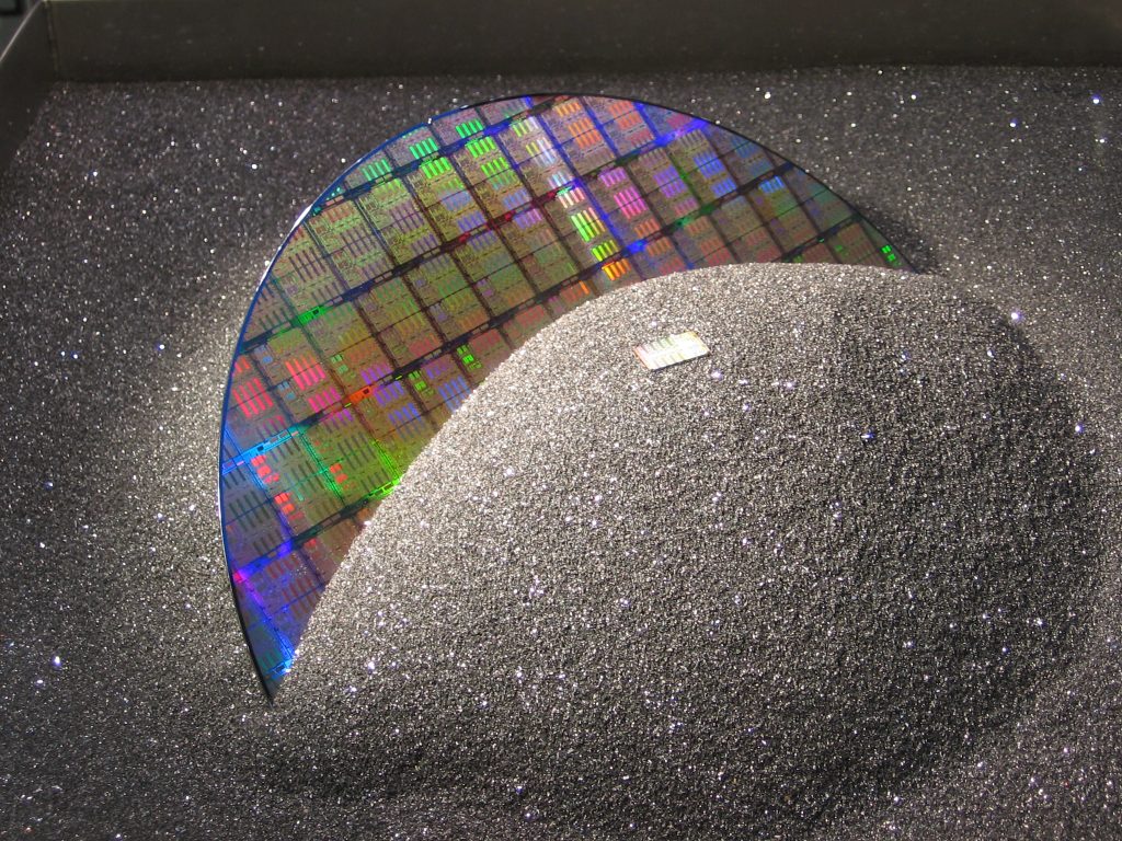
substrate in semiconductor production.
With the goal of enhancing the reliability and performance of microelectronics in the face of radiation challenges, Laboratory Directed Research & Development researchers have made significant strides in developing non-volatile, radiation-hard ferroelectric memory using innovative materials such as hafnium oxide and hafnium zirconium oxide. This advancement is being integrated into Sandia’s trusted radiation-hardened fabrication facility, specifically within the MESA CMOS technology.
The team is focused on creating a robust backup technology that ensures the availability of reliable microelectronics in a global landscape where supply is limited. By achieving a higher level of radiation hardness, Sandia aims to fill a critical technology gap for national defense systems that require durable, non-volatile memory solutions. The integration of ferroelectric memory into existing processes not only mitigates risks associated with future developments but also positions Sandia at the forefront of semiconductor technology.
This work has pushed ferroelectric memory with FeRAM at the 200 mm wafer scale and generated both binary and 32-state ferroelectric tunnel junctions, demonstrating advanced capabilities in memory device engineering. Sandia researchers are actively testing and characterizing these new materials to understand their performance under radiation exposure. This work has already been showcased at a conference, highlighting its significance in advancing the field.
Looking ahead, Sandia plans to advance this research with follow-on projects aimed at developing supporting circuitry for the ferroelectric memory cells, further solidifying its commitment to innovation in microelectronics.
May 13, 2026