Advancing memory technologies through strategic partnerships
Recent advancements in memory technology have reached a significant milestone through a partnership between Sandia and Intel. The Advanced Memory Technology program has successfully evolved early research and development into a novel memory capability by leveraging existing dynamic random access memory technology alongside innovative techniques.
Led by Sandia, and in collaboration with Lawrence Livermore and Los Alamos national laboratories, the AMT program establishes strategic partnerships with industry to address memory bandwidth and latency limitations in critical NNSA mission applications. The program is funded through the Advanced Simulation and Computing program as part of a post-exascale initiative.
“As the performance of computational units and memory subsystems have continued to diverge over the last decade, the ability of the NNSA to speed up its mission critical applications has become more challenging,” said Si Hammond, program director for Advanced Computing at the NNSA. “We are on a constant search for higher performing memory technologies to help meet important mission goals.”
The Tri-lab and Intel partnership has taken place over the last few years. Rounds one and two focused on research and development, while the third round will target productization. Those early investments are now making the R&D real.
“Intel’s Next Generation DRAM Bonding initiative has demonstrated a novel memory architecture and revolutionary assembly methodology that significantly increases DRAM performance, reduces power consumption, and optimizes memory costs,” said Joshua Fryman, CTO of Intel Government Technologies. “Standard memory architectures aren’t meeting AI needs, so NGDB defined a whole new approach to accelerate us through the next decade.”
Today, systems that use high bandwidth memory exchange improved bandwidth for lower performance in other metrics such as capacity. NGDB eliminates much of the tradeoff between high bandwidth and double data rate DRAM while significantly improving energy efficiency over both. In doing so, NGDB allows a broader set of applications and systems to take advantage of higher bandwidth memory.
Gwen Voskuilen, principal member of technical staff at Sandia, said, “This is an exciting technology that we anticipate will lead to a wider adoption of higher bandwidth memories in systems that are currently unable to take advantage of high bandwidth memory due to its limited capacity and power constraints.”
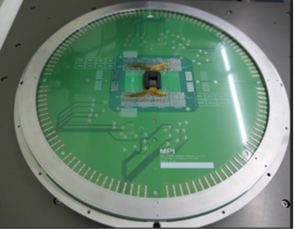
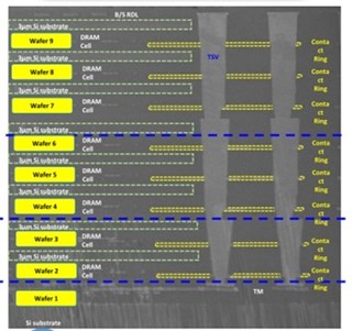
Under the initiative, both a novel stacking approach as well as a new DRAM organization were developed. While initial prototypes confirmed the viability of the novel assembly method for overcoming memory capacity limitations in current technology, the latest prototype demonstrates functional DRAM using the new stacking approach. “The demonstration confirms that the NGDB technologies can be combined to yield a highly performant memory with high-volume manufacturing,” said Voskuilen.
AMT is a driving force in strengthening these types of trusted technology partnership, allowing the U.S. to lead in foundational semiconductor technologies and enable global deployment of emerging capabilities that’s research begins in a national laboratory.
“This is the ideal outcome for the AMT program,” said James H. Laros III, Senior Scientist and AMT program lead. “Partnering with commercial entities in advanced research and development that leads to the availability of a real capability that can benefit the ASC mission and furthers computing research.”
January 8, 2026