
Sandia National Laboratories announced a continued collaboration with AMD as part of the NNSA’s Advanced Simulation and Computing Advanced Memory Technology (AMT) program.
This collaborative research and development agreement, led by Sandia in partnership with Lawrence Livermore National Laboratory and Los Alamos National Laboratory, will work with AMD to investigate advanced packaging techniques for semiconductors.
The research looks at advanced packaging, the methods used to connect and stack chips, and how these techniques can create performant, power‑efficient, scalable systems. Today’s systems can slow down because processors and nearby memory cannot store and transfer enough data efficiently. Packaging improvements that increase on‑chip storage and techniques that improve data movement efficiency can boost performance and reduce power use for high‑performance computing and artificial intelligence.
Using advanced packaging comes with challenges, including managing heat and physical stress on the chip and package. By addressing these issues, the research could improve next‑generation GPU designs and open new possibilities in artificial intelligence, scientific modeling and other large‑scale computing workloads.
“Advanced packaging helps us place memory closer to the processor by stacking chips and connecting them more tightly, so larger memory feels nearby. That can speed up supercomputing and large AI models while using less power. The challenge is keeping these tightly packed systems reliable by controlling heat and physical strain” said Ben Feinberg, a principal member of the technical staff at Sandia National Laboratories.
“Creating faster access to larger pools of memory has been one of the great challenges in computer architecture,” said Si Hammond, Program Director for Advanced Computing at the NNSA. “We are delighted to continue partnering with AMD to use these advances to power future generations of NNSA’s high-performance computers and AI infrastructure.”
Memory bandwidth has long been a bottleneck in modern high-performance computing. As processors and accelerators advance, moving data efficiently between memory and compute increasingly determines simulation throughput and energy use for large-scale modeling.
“AMD is proud to deepen our long-standing collaboration with the Department of Energy’s national laboratories as we push the boundaries of memory and packaging technologies for high‑performance computing and AI,” said Ralph Wittig, corporate vice president and head of Research and Advanced Development at AMD. “By working closely with Sandia, Lawrence Livermore and Los Alamos, we can align our next‑generation GPU and memory architectures with the demanding needs of mission‑critical workloads.”
This collaboration will help support the next-generation of GPU designs to unlock new capabilities in artificial intelligence, scientific modeling and other data-intensive workloads.
“The ASC has a long history of research and development partnerships with AMD, leading to deployments such as Red Storm at Sandia National Laboratories and El Capitan at Lawerence Livermore Laboratory. Continued public-private partnerships like these are essential to influencing future technologies that support the ASC mission,” said Sandia senior scientist and AMT program lead James H. Laros III.
The contract supports continued innovation in advanced memory technology and strengthens engagement between the national laboratories and U.S. industry to help deliver future high-performance computing capabilities for critical research challenges and national security.
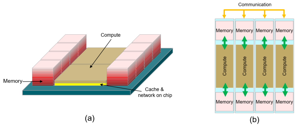
(b) Spatial locality techniques place data and associated compute in localized partitions to reduce data movement distances, improving energy efficiency and paving the way for further integration opportunities such as 3D stacking of memory. (Graphic courtesy of AMD).
October 12, 2026