Sandia employs integrated photonics as solutions for quantum technology for communication, sensing, computing, and networking
Photonics for Chip-scale Quantum Devices
Sandia National Laboratories has full silicon and compound semiconductor photonic integrated circuit fab capability and broad quantum phenomenon expertise that includes an Ion Trap Foundry and Quantum Computing Test Bed (www.sandia.gov/quantum). We use a suite of application-specific quantum photonic integrated circuit (QPIC) technologies to shrink the optical tables that interface with the quantum world to chips that perform the same function. Sandia is a quantum device realization center and our partners and collaborators can leverage our capabilities.
Key Capabilities
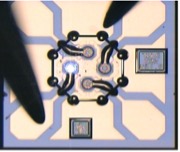
- Ionic qubits using surface electrode ion traps with integrated photonic waveguides, light delivery, and integrated on-chip modulators; solid state diamond vacancy centers
- Silicon photonics, low loss alumina waveguides, cryogenic modulators, frequency combs, Ge on Si single photon avalanche detector, heterogeneously-integrated lasers
- Narrow linewidth lasers, amplifiers, cryogenic modulators, and detectors
- Visible, UV and NIR capability, low loss waveguides, thermo-optic modulation, cryogenically-compatible piezoelectric modulation, detectors, heterogeneously-integrated lasers, acousto-optics
- Narrow linewidth VCSELs
Example Applications
Quantum Sensing
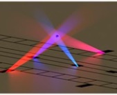
Miniaturized Atom Interferometers
Atom interferometers in large laboratory systems achieve unrivaled inertial sensing capability. In order to be relevant for most applications, atom interferometry systems must be small and portable. Sandia developed technology to shrink these systems by orders of magnitude to the size of a shoe box. One critical development is a quantum photonic chip. Sandia developed silicon integrated photonics (SIP) suppressed-carrier single-sideband (SC-SSB) modulators with a dual-parallel Mach-Zehnder configuration and four phase modulators at each path. The SIP modulators dynamically tune a light frequency during the measurement sequence to demonstrate state-selective atom detection for atom interferometry.
Atomic Clocks
Sandia develops low power narrow linewidth VCSELs for chip scale atomic clocks. This technology has been transferred to industry and is incorporated in commercial chip scale atomic clock products that use Cesium vapor cells (see https://newsreleases.sandia.gov/atomic-clock).
Sandia also develops quantum photonic integrated circuits (QPICs) for addressing trapped ion atomic clocks. These QPICs deliver the multiple diverse wavelengths on a chip needed to ionize, cool, excite, pump and interrogate trapped ions (see https://www.sandia.gov/quantum/Projects/tictoc.html)
Quantum Communication
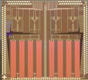
Quantum Key Distribution Chips
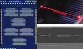
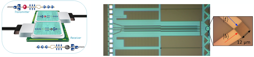
A Sandia research team developed and demonstrated the first microfabricated quantum transmitter/receiver called T-QUAKE (Transceiver for Quantum Keys and Encryption), and received a 2016 R&D 100 Award for this accomplishment. The system miniaturizes all the components necessary to securely encode, transmit, receive, and decode quantum photonic signals onto a single microchip, in effect creating an ultra-secure cryptographic network node for any secure communication or network application. T-QUAKE accomplishes what bench-scale quantum encryption systems do but at one millionth the scale, on a chip roughly 3 mm x 5 mm and weighing less than an ounce. These silicon photonics quantum key distribution encoder chips operated in an intercity metropolitan field test (Boston) over 43km of fiber at a composable secret key generation rate of 157 kbps.
Because of the ability to mass fabricate microchips using traditional CMOS techniques, T-QUAKE also dramatically reduces costs. Current quantum communication laboratory systems have a price point greater than $100,000 for one transmitter-receiver system. We estimate that Sandia’s chips could cost less than $5,000 per transceiver in existing, high-consequence cyber and physical security markets and less than $100 per transceiver when mass produced for future commercial electronics markets, transforming quantum communications from the national laboratory research realm to the military-industrial domain and, soon, consumer laptops and mobile phones.
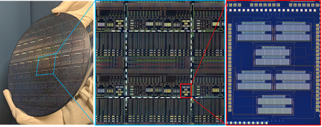
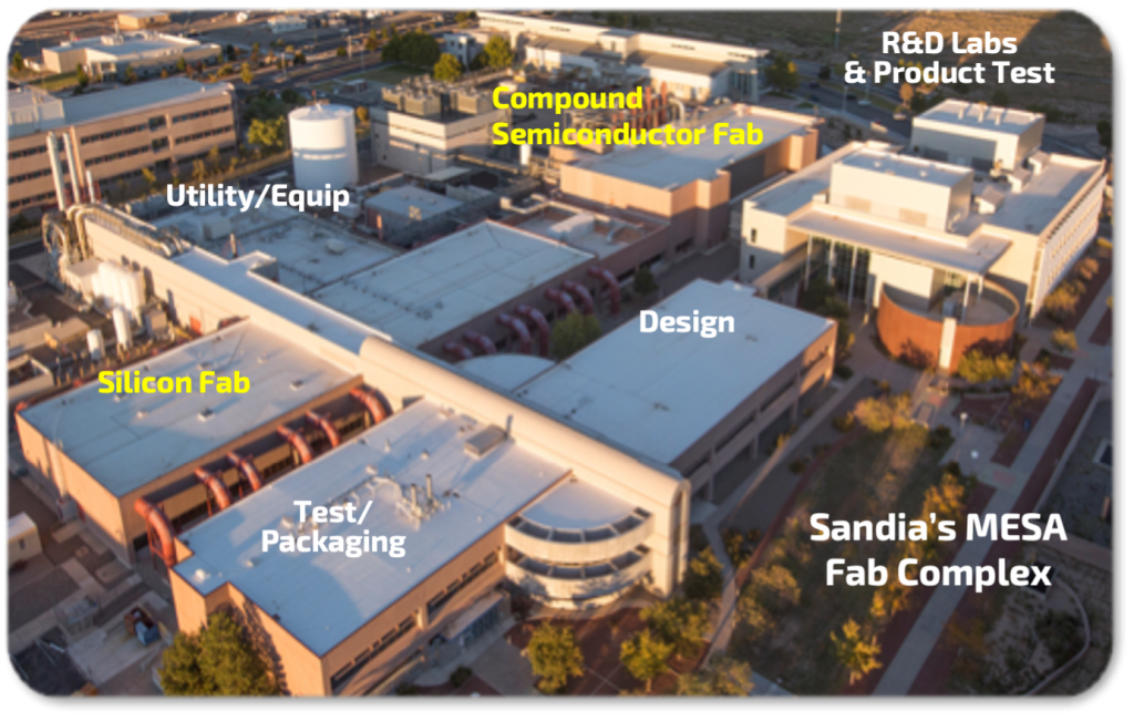
Quantum Integrated Photonic Foundry Capabilities at Sandia’s MESA facility
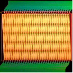
Sandia National Laboratories has developed an integrated photonics portfolio to enable quantum-on-a-chip for applications including qubits, atomic clocks, and atom interferometers, leveraging decades of research in microelectronic and photonic research and advanced prototyping and production capabilities. Sandia’s National Security Photonics Center (NSPC) offers collaborative multi-project wafer (MPW) runs in Silicon Photonics (200 mm) and InP photonics, and leverages this capability for quantum applications.
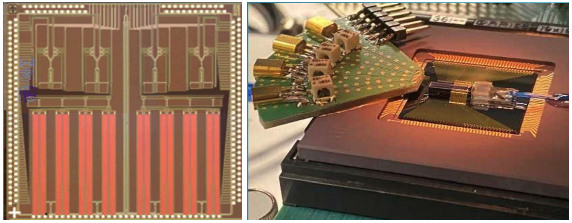
Sandia’s quantum photonics portfolio contains a wide variety of component and platform technologies. Our standard Silicon photonics Si-on-SOI device library has over 50 passive and active devices, and the customizable capability in our quantum photonics portfolio includes 1) additional SiPh components that operate below 2K, 2) low-loss SiN and alumina waveguide platforms, 3) a broad range of heterogeneously integrated components ranging from III-V hybrid lasers, integrated III-V GaN, GaAs, and InP lasers and amplifiers, 4) MEMS acousto-optics and Si/SiN nano-optomechanics, 5) bonded LiNbO3, 6) optical isolators, 7) an in-plane GaAs platform with narrow linewidth lasers, amplifiers, and cryogenic modulators, 8) advanced single photon sources in diamond, 9) superconducting detectors and Josephson junctions. Furthermore, Sandia has developed extensive electronic and optical packaging for rapid prototyping.
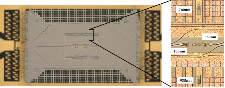
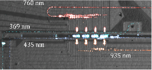
The broad capability of the NSPC developed over many past and active projects has led to many world-first / world-class devices and demonstrations. To illustrate, we demonstrated on-chip quantum key distribution (QKD) transceivers that encode quantum information in the polarization state of a single photon or the amplitude and phase quadratures of a photonic coherent state. Photonics are actively enhanced with new integrated waveguide materials in the visible and ultraviolet (UV) spectral range. New III-V optoelectronic devices such as narrow linewidth lasers operating at 778 nm and 369 nm for integrated ion trap clocking, and electro-absorption modulators at 760 nm working at cryogenic temperatures. Novel materials integrated into advanced CMOS process flows for acousto-optic transduction device development have a long history at Sandia. Advanced AlN piezoelectric devices have successfully operated at cryogenic temperatures and are being exploited for quantum transduction from microwave to the visible and (UV) spectral range. Flexible materials offer high extinction high speed switches, and acousto-optic frequency shifters and can be integrated with quantum emitters such as diamond.
Sandia’s extensive quantum photonics platform provides a customizable portfolio of tried and tested photonic building blocks, a baseline platform with a powerful process and design kit (PDK), and flexible fabrication processes to create new and innovative quantum microsystems for science exploration. Sandia’s advanced in-house optical and electrical packaging and heterogenous integration capability puts new co-designed devices for advanced quantum photonic applications in researchers’ hands for testing.
Quantum Photonics Technologies in Sandia’s Portfolio.
- On-chip material platforms
- Telecom bands: Si, InP, InGaAs, AlN
- Visible low-loss: SiN, AlN, III-V, Al2O3
- Ultraviolet: Al2O3,III-N (GaN-InGaN)
- Atomic Layer Deposition (Thin nitrides and oxides HfO3)
- Bonded LiNbO3
- Diamond with implanted vacancy centers.
- Superconducting films: Nb, NbN, Al, & compatible insulators NbO, Al2O3
- On-chip splitters and routing:
- Directional couplers
- MMI splitters
- Add-Drop routers & Ring filters
- Star-couplers and arrayed waveguides (AWG)
- MZI switches
- Thermo-optic switches
- Polarization splitters and rotators
- Polarization splitting grating
- On-chip active devices (building blocks)
- High extinction amplitude modulators (MZI, electro-absorption, ring, and disk)
- Low-loss phase shifters
- Piezoelectric AlN transducers
- Lasers & amplifiers: GaN, GaAs, InP, GaSb (ex. narrow linewidth @ 369 & 778nm, 1550 nm)
- Ge on Si high speed pin detector
- Ge on Si Avalanche photo detector (Single photon)
- Silicon single photon avalanche photodiodes (SPADs)