A miniature, highly mobile optical atomic clock enabled by integrated single-photon detectors and waveguide light delivery.
Critical Need
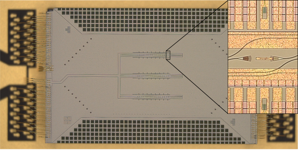
Position, Navigation, and Timing (PNT) are critical capabilities to DoD missions as well as for many civilian applications. Currently, PNT resources are primarily provided by the Global Position System (GPS), however recent technology has made GPS vulnerable to disruption. Providing a local and transportable timing source will give redundancy to GPS in the event of a service outage. The precision of an optical atomic-clock is required to meet the timing needs, however scaling down the bulky laboratory infrastructure required to control the atoms poses significant challenges. This is one of the key goals of DARPA’s A-PhI program, which funds our project named Trapped Ion Clock with photonic Technologies on Chip (TICTOC). TICTOC will take advantage of novel atomic interrogation protocols on ensembles of individually localized atomic ions. The microfabricated surface ion-traps developed at Sandia offer an ideal platform for transportable optical atomic clocks: photonics integrated directly in the surface trap can control and deliver light precisely to each atom and single-photon detectors can be fabricated directly under each atom for individual readout. The individual addressability and readout of the atoms is a key capability that allows us to significantly reduce resource and size requirements for our transportable optical atomic clock.
Project Innovation
Probing the optical frequencies of atoms requires precise localization of the atoms and precise control and measurement of their electronic state. An ion trap platform is not only well suited for confining individual atomic ions, but it can also provide the platform and the photonics that are required to deliver light to control the ions and the detectors for state readout. Because of the precision and scalability of the fabrication process, we can individually trap, address, and detect 10’s to 100’s of ions. This allows us to use more advanced clock-interrogation schemes (multi-ensemble interrogation) that can offer dramatic improvements to the overall clock performance. Our collaborators at NIST have shown that the multi-ensemble interrogation approach can give an exponential improvement to clock stability.
Integrated Single-Photon Avalanche Detectors (SPADs)
In most atomic physics systems, detection of the atom’s state is accomplished with resonance fluorescence using macroscopic equipment such as bulk lenses and commercial single-photon detectors, both placed outside the vacuum chamber. For experiments involving only a single or a few atoms this detection scheme works well, but when 10’s or higher number of atoms are involved the limitations of this detection scheme, such as crosstalk and individual distinguishability, become apparent. Additionally, for applications requiring mobility, bulky external optics lead to operational fragility and high size, weight, and power (SWaP) requirements.
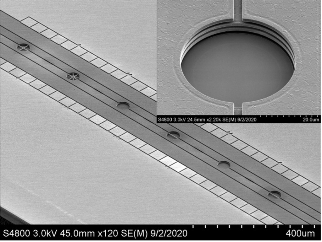
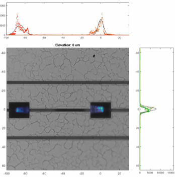
The solution is to integrate detectors into the vacuum apparatus and place them as close to the atoms as is reasonably possible. We have demonstrated the first SPADs integrated into a surface ion trap, detecting 369 nm fluorescence from ytterbium ions, accomplished at room temperature. Future TICTOC traps will incorporate dozens of integrated SPADs, allowing us to carry out the multi-ensemble protocol to achieve excellent clock stability.
Integrated waveguides for light delivery
For similar reasons it’s desirable to integrate detectors into ion traps, integrated waveguide delivery of light to trapped ions is crucial to experimental robustness and low SWaP performance of fieldable systems. Externally delivered laser beams suffer from positional instability over time and require significant volume, making them not suited for mobile applications. We have demonstrated quantum operations with ytterbium ions at a record-low ion height of 20 microns with no measurable additional heating due to the waveguide output couplers. We have fabricated traps with integrate waveguides capable of delivering all necessary wavelengths beams, which will be a key component of future TICTOC traps containing both integrated waveguide delivery optics and integrated SPADs.
Miniature Microwave Ion Clock
In a significant advancement for atomic clock technology, researcher Daniel Thrasher (5228) is leading efforts to create miniature microwave ion clocks with enhanced reliability and precision, both qualities of which are crucial for national security and defense applications.
Thrasher’s miniature microwave ion clocks utilize buffer gas-cooled ytterbium or barium ions confined in radio frequency traps, allowing them to maintain accurate time. A recent study highlights the impressive long shelf-life of miniature vacuum chambers designed to store these ions, demonstrating that they can remain functional for decades.
This breakthrough in quantum sensing technology is particularly important for critical applications such as GPS and telecommunications, both of which are vital for military operations and national defense strategies. Improvements in timekeeping technology boost navigation, communication, and overall safety in various applications. On an individual level, Thrasher’s work helps to ensure that systems we rely on every day, such as GPS for driving and telecommunications for connecting with others, operate smoothly and efficiently. From a national security perspective, accurate timekeeping in challenging environments, including outer space and vital infrastructure, is crucial.
Drifts in timekeeping threaten the precision of navigation systems, the effective encryption and decryption of messages in communication networks, data integrity, coordination of military operations, and the successful synchronization of surveillance and reconnaissance activities. Thrasher’s miniature microwave ion clocks aim to address these threats posed by drift in timekeeping. His advancements not only enhance the reliability of defense systems but also strengthen the nation’s overall security framework.
Surface trap design and fabrication
Sandia has been designing and fabricating surface ion traps for over two decades using an in-house R&D fabrication capability that supports experiments in research programs in quantum computing, quantum simulation, quantum sensing, and atom optical clocks. Our surface trapped ion quantum device capability leverages decades of research in microelectronics, micro electromechanical systems (MEMS) and integrated photonics, and is equipped with device prototyping, advanced packaging, and heterogeneous integration capabilities. Sandia has delivered defect-free, fully packaged, experiment ready ion traps to leading quantum information science research efforts, including Sandia-led, academic, and commercial groups in the United States and Europe, where numerous ground-breaking quantum information science experimental breakthroughs have been demonstrated.
TICTOC-funded publications
- Ivory et al., “Integrated optical addressing of a trapped ytterbium ion”, submitted to Phys. Rev. X. arXiv version.
- J. Setzer et al., “Fluorescence Detection of a Trapped Ion with a Monolithically Integrated Single-Photon-Counting Avalanche Diode”, submitted to Appl. Phys. Lett. arXiv version.
- E. Kim et al., “Multi-ensemble clock algorithm for probing beyond the laser coherence time”, in progress
- O’Mally et al., “Optical Dual-comb Vernier Division of an Octave-Spanning Kerr Microcomb”, CLEO 2021
- H Lai et al., “871-nm Ultra-Narrow-Linewidth Laser for Yb+ Clock”, CLEO 2021
TICTOC Key Contributions
- First demonstration of trap-integrated single-photon avalanche detectors. Performed at room temperature.
- Lowest published ion height (20 μm) in surface ion trap.
- Experimental realization of the multi-ensemble clock protocol.
- Lowest phase-noise laser at 871 nm for Ytterbium ion clock operation.
- Demonstration of novel “Vernier” micro-fabricated frequency comb.
- Record on-chip doubling efficiency for 871 nm to 435 nm optical conversion.
Partners
Sandia leads the TICTOC project which includes four other contributing teams.
- Leibrandt group, NIST Boulder. Algorithm development and proof-of-principle experiments.
- Weiner group, Purdue University. Novel micro-fabricated frequency comb development.
- Tang group, Yale University. Integrated second-harmonic crystal and integrated optical amplifier development.
- OEwaves Inc. Low-noise local oscillator development.
Contact
Please contact us at tictoc@sandia.gov