R&D 100 Awards
2013
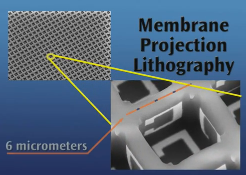
R&D100 Entry 2013: Membrane Projection Lithography
This fabrication technique enables the creation of a diverse array of microscopic 3D structures with macroscopic impact. For instance, the technique can be used to create 3-dimensional integrated circuits, the next step in the evolution of 2-dimensional microprocessors. It is also capable of creating structured electromagnetic materials. Currently, the technique is being used to make thermal antennas which can control the direction of heat emitted from an object, potentially easing cooling and heating needs for satellites or perhaps even buildings and cars.
Watch R&D100 Entry 2013: Membrane Projection Lithography
2012
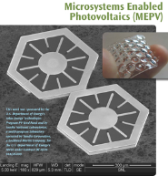
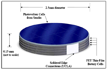
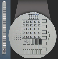
Microsystems Enabled Photovoltaics wins 2012 R&D 100 Award (23 MB PDF)
Sandia developed tiny glitter-sized photovoltaic (PV) cells that could revolutionize solar energy collection. The crystalline silicon micro-PV cells will be cheaper and have greater efficiencies than current PV collectors. Micro-PV cells require relatively little material to form well-controlled, highly efficient devices. Cell fabrication uses common microelectronic and micro-electromechanical systems techniques. They are 10 times thinner than conventional cells, yet perform at about the same efficiency.
Video: R&D100 Entry 2012: Breakthrough: micro-electronic photovoltaics
Video: Microsystems Enabled Photovoltaics
2011
R&D100 Entry 2011: Microresonator Filters and Frequency References (8 MB PDF)
Our miniature acoustic resonators perform RF filtering and frequency synthesis in next-generation wireless devices—offering higher performance in a smaller package with a lower price.
Our microresonators are miniature acoustic resonators fabricated using complementary metal-oxide semiconductor (CMOS)-compatible microfabrication techniques. When grouped together, our microresonators operate as filters; they provide frequency selection in radios and other electronic equipment. When connected with transistor electronics, microresonators can provide frequency reference functions (such as clocking) to radios, microprocessors, and other electronic devices.
Video: R&D100 Entry 2011: Microresonator Filters and Frequency References
2010
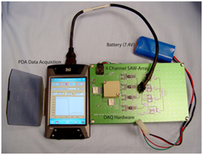
Acoustic Wave Biosensor for Rapid-Point-of-Care Medical Diagnosis (6 MB PDF)
The device, a joint effort of Sandia Labs and the University of New Mexico Health Sciences Center, is essentially a handheld, battery-powered, portable detection system capable of identifying a wide range of medically relevant pathogens from th eir biomolecular signatures. Detection can occur within minutes, not hours, at the point of care, whether that care is in a physician’s office, a hospital bed, or at the scene of a biodefense or biomedical emergency. According to the researchers, “The Acoustic Wave Biosensor provides fast, low-cost diagnostic results with as good or better sensitivity than traditional techniques.” The device’s sensor array works like a miniature analytical balance, weighing the amount of pathogen that binds to its surfaces. The pathogen-bound sensor acts like a spring with a small weight bouncing at one end. As more pathogens stick to the surface, the weight on the spring increases, causing the spring’s bouncing speed to decrease by a measurable amount. The sensors detect minute weight differences by this method. A variety of sticky substances (ligands) attach to different pathogens. Surface tension draws the sample over the sensor, so no pumps or valves are required. This makes the sensors smaller, more reliable, less expensive to manufacture, and the process extends the operating time of the rechargeable batteries. System control, data analysis and reporting are performed by a personal digital assistant (PDA).
Video: R&D100 Entry 2010: Acoustic Wave Biosensors for Rapid Point-of-Care Medical Diagnostics
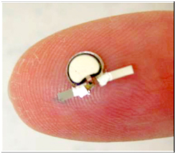
Micro Power Source (3 MB PDF)
You’ve accepted that batteries run out of power and that newer batteries are rechargeable in wall electric sockets. But why should you go through all that? Why not a battery covered by a thin photovoltaic film? Just like on rooftops, the photovoltaic surface could harvest sunlight and turn it into electricity, recharging the battery in an ongoing process. This work, joint with Pacific Northwest National Laboratory and Front Edge Technology Inc. in Baldwin Park, Calif., was originally part of a Defense Advanced Research Projects Agency program, but commercial applications were “evident from the start,” the researchers wrote.
The most likely immediate applications of the durable batteries are self-powered environmental sensors, self-powered tags for material tracking, and self-powered ‘smart’ cards to enhance user features and security. The key feature for the micropower source is a volume of only one microliter, yet a high peak-power density greater than 1,000 watts per liter. This makes the device useful for powering wireless microsystems that sense, record, transmit and/or actuate. The photovoltaic battery stack itself is only five millimeters in diameter and approximately 50 microns thick. (A human hair is approximately 70 microns thick.)
Video: R&D100 Entry 2010: Micro Power Source
2009
ltralow-Power Silicon Microphotonic Communication Platform (3MB PDF)
An ultra-low-power microphotonic communications platform made of silicon, for wavelength division multiplexed communications within high performance computers. The ultrasmall components establish a platform of elements capable of addressing the bandwidth and power consumption problems of high-performance computer and data communications networks. Silicon resonant modulators demonstrate for the first time 100-microwatts/gigabit/second optical data transmission on a silicon CMOS-compatible platform. Together with the first high-speed silicon bandpass switches, the platform enables optical data transmission and routing on a silicon platform at nanosecond switching speeds with up to 100-times less power consumption and 100 times the bandwidth density compared to traditional electronic approaches.
Video: R&D100 Winner 2009: Ultralow-Power Silicon Microphotonic Communications Platform
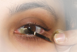
Artificial Retina
Sandia shares a part of this award for moving research forward to enable the blind to see. The project employs a small video camera on a patient’s glasses sending images to a compact image processor on the patient’s belt. The processor commands an implant to deliver the desired pulse of current to an electrode array attached to the patient’s retinal tissue. This inner-eye array stimulates the retinal tissue nerves which ultimately connect to nerves leading to the visual cortex of the brain where the patient sees an image. The award was given to a multi-lab/industry collaboration funded by DOE, initiated by Oak Ridge National Laboratory, and submitted for an award by Lawrence Livermore National Laboratory. Sandia is developing MicroElectroMechanical Systems (MEMS) and high-voltage subsystems for advanced artificial retina implant designs. These include microtools, electronics packaging, and application-specific integrated circuits (ASICs).
Video: R&D100 Winner 2009: Artificial Retina
Video: LLNL video
2008
Silicon Micromachined Dimensional Calibration Artifact for Mesoscale Measurement Machines
Designed to help improve measurement accuracy for miniaturized devices, such as fuel injectors, watch components, and inkjet printer parts. The Sandia MEMS-based three-dimensional physical artifact is 10 times more accurate and much less expensive than the former gold standard and can be used to calibrate a variety of inspection systems.
2007
Self-Assembling Process for Fabricating Tailored Thin Films (4MB PDF)
Project involved development of a simple soft coating process that forms optical, electrical, and magnetic thin films from self-assembled nanoparticles. Researchers developed a wet-solution-based process employing self assembly to create engineered nanocomposite thin films with tunable properties by varying particle composition, sizes, shapes, and particle packing density and geometry.
ElectroNeedle™ Biomedical Sensor Array (1MB PDF)
Designed to help improve measurement accuracy for miniaturized devices, such as fuel injectors, watch components, and inkjet printer parts. The Sandia MEMS-based three-dimensional physical artifact is 10 times more accurate and much less expensive than the former gold standard and can be used to calibrate a variety of inspection systems.
Older R&D 100 Awards
Global-Link Sandia used innovative data compression techniques to help physicians consult in real time over MRI pictures, though the amount of data transferred is normally huge and the healers may be thousands of miles from each other. Global-Link allows such rapid transmission of complex data that a doctor in the U.S. can confer with a doctor halfway around the world, viewing and manipulating 3-D MRI imagess in real time directly on each doctor’s MRI computer. Similarly, oil team members can confer around the globe on observed data. So can military commanders. Extremely responsive interactions between an event and a remote, secure, high-resolution display are possible using Global-Link across the Internet. Results were achieved in collaboration with Logical Solutions, Inc., which is marketing the product.
Ion Photon Emission Microscope-IPEM A patented exploratory ion beam microscope system that does not require costly and complicated forming and focusing equipment. The system was invented and patented by, jointly with Quantar Technologies, which is marketing this invention. The multidimensional, high-resolution analysis system is called the Ion-Photon Emission Microscope (IPEM). It allows scientists and engineers to microscopically study the effects of single ions in air on semiconductors, semiconductor devices, and biological cells without having to focus the beam. The technique determines the position at which an individual ion enters the surface of a sample; thus, focusing a beam is unnecessary.
traffic lights. A national initiative is now underway to develop solid-state sources for high-efficiency white lighting. The cantilever epitaxy process of growing LEDs may help meet those needs. Over the past several years LEDs have been grown with various combinations of gallium nitride alloys on sapphire substrates. However, the atoms of the two materials do not line up perfectly due to differences in natural lengths of the bonds in their respective crystal lattices. Regions of imperfections, called dislocations, accompany this lattice mismatch. These dislocations limit LEDs’ brightness and performance. The new cantilever epitaxy process reduces the numbers of dislocations, giving the potential for longer-lived and better performing LEDs. It also means that LEDs grown on the patterned sapphire/gallium nitride substrates can produce brighter, more efficient, green, blue, and white lights than previously accomplished. Because of the reduction in dislocations, the cantilever epitaxy process shows “great promise for making a superior substrate for light-emitting devices” and has potential for applications to a wide variety of electronic devices and GaN integrated circuit technology. Transmission electron microscopy (TEM) and scanning electron microscopy (SEM) is used to determine the amount of dislocations eliminated through the cantilever epitaxy process.
Turn Off (ETO) Thyristor Lightning strikes, equipment failures, or other anomalies in electric powered transmission systems can cause brown-outs or even network failures. But a fast-response semiconductor device allows a utility to rapidly convert energy stored in a DC device into AC power and minimize the negative effects of such interruptions on electrical devices. Under the auspices of the DOE Energy Storage Systems Program, The advanced semiconductor unit called an ETO (emitter turn-off thyristor), is a three-terminal semiconductor device similar to a MOSFET (metal oxide semiconductor/field effect transistor) but capable of switching greater power at high frequencies. The ETO, rated at 4000A and 4500V, can switch power at 1-3 kHz. The ETO R& D 100 application was a joint entry with Solitronics (a Blacksburg small business marketing the ETO), Virginia Tech (ETO inventor), Sandia (which supported the development of the ETO from a concept to an actual product suitable for utility energy storage applications), and the American Competitiveness Institute in Philadelphia (which assisted the team with manufacturing engineering and prototype production of the device).
Extreme UV Lithography Full Field Step-Scan System Editor’s Choice Award, in addition to R&D 100 recognition. The award is “for the Greatest Improvement Upon an Existing Technology” and one of three technologies considered by R&D Magazine editors to be the most outstanding achievements among the 100 selected. More than 50 Sandians and collaborators from Lawrence Livermore (LLNL) and Lawrence Berkeley national laboratories were honored for this technological advance that will lead to dramatic improvements in the speed and memory of computer systems. They created the only system that can pattern full chip-size areas on silicon wafers with features as small as 50nm. It is the embodiment of a set of groundbreaking technologies that were considered by many to be impossible as recently as a few years ago. Commercialization of this breakthrough will allow advances in microelectronics to continue into the next decade. In addition to the national laboratory team, the award is also being given jointly to Northrop Grumman Space Technology/Cutting Edge Optronics. The work was done in partnership with an industrial consortium comprising Intel, Motorola, AMD, Infineon, IBM, and Micron. Intel ordered the first production-level instrument based on this technology last year.
MEMS Based Adaptive Optics Phoropter (MAOP) Sandia contributed to the opto-mechanical design and integration of a compact, transportable adaptive optics system that expands upon traditional devices currently used in optometrists’ offices. In addition to determining correction needed for near-sightedness or far-sightedness and astigmatism, it also determines correction needed for high-order aberrations that can interfere with night vision and can provide a preview of correction to a patient. The effects of aberrations can be compared to distortions seen in a pool due to ripples on the surface. Diminished night vision or a perception of “halos” can sometimes result from aberrations introduced during laser eye surgery. The Adaptive Optics Phoropter is a system that uses MEMS-based deformable mirror technology to correct wavefront aberrations in the eye. It combines technologies from astronomy and micromachining to advance the study and treatment of retinal diseases. Applications for the tool include generation of improved prescriptions for custom contact lenses or laser eye surgery, as well as high-resolution retinal imaging. The award is shared by LLNL, which led the project, Sandia, the University of Rochester, Wavefront Sciences, Boston Micromachines Corp., and Bausch & Lomb.
SnifferStar Chemical Sensor SnifferStar™ mounts on a drone aircraft for remote surveillance of battlefield situations where suspect plumes or clouds are present. The detector’s primary purpose is to save lives by warning soldiers that chemical weapons are present on a battlefield. Developed under a Shared Vision program with Lockheed Martin, the entire module weighs less than a golf ball, operates on less than 0.5 watts, and uses the wind generated by the motion of the craft to collect samples for analysis. SnifferStar is sensitive to both blister and nerve agents. It ignores common interferents and analyzes chemical warfare agents in 20 seconds. The device also has possibilities for use in or near the ventilation systems of buildings, or, with addition of small pumps to force air into the device, on posts surrounding military bases.
MTR8500 Very Short Reach (VSR) OC-192 Parallel Array Transponder Module The MTR8500 is the first commercial fiber optic transponder to use 12-channel, 1.25 gigabit per second transceivers coupled to 12-channel fiber ribbon cable for short haul applications. This parallel channel approach, enabled by microsystems inventions in optical transceivers, flexible circuit boards, optical power control, optoelectronic housing & mounting, and optical coupling has resulted in a transponder that can be manufactured for 1/10 the cost of other products. The project, funded by EMCORE Corporation, and was submitted by Sandia as a joint entry with EMCORE’s Fiber Optics Division of Albuquerque.
Ion-Induced Electron Emission Microscope (IEEM) System A new way to perform ion beam analyses without having to focus the high-energy ion beam. The IEEM was a joint entry between Sandia and Staib Instruments, Inc., Langenbach, Germany. Staib is now manufacturing the IEEM.
Solid State Radiation Materials and Detectors A team of researchers developed a new technique of growing large single crystals of cadmium zinc telluride (CZT) suitable for radiation detectors. The new solid-state radiation detectors are unique because they can operate at room temperature, detect X- and gamma-ray radiation with high efficiency, and uniquely identify the isotopes responsible for the emitted radiation. The team’s development of an improved technique to grow detector-grade CZT crystals and a new method to reduce the dark current flowing along the crystal surfaces have allowed for major improvements in the signal-to-noise ratio, long-term stability, and yield of single-crystal material. The technique was developed by Sandia; Yinnel-Tech Inc. in South Bend, Ind.; Techion, Israel Institute of Technology; and Fisk University.
Other Awards
- MESA MLAB – LEED Silver
- MESA WIF – LEED Silver
- MESA MicroFab – LEED Certified (1st LEED Green Microchip Fabrication Facility in the world)
- CINT – LEED Certified
- Champion of the Year – Gilbert V. Herrera
- JCEL – LEED Silver
* Electroneedle Array (Nomination)
* MESA Project
- Champion of the Year – Dale L. Hetherington
- Black Belt of the Year – Amy Moy
- Green Belt of the Year – Jonathan W. Wittwer
- 2013 – Sandia Labs names three fellows
- 2011 – Solar glitter, rescue robot
- 2007 – Bio-threat detection
- 2007 – Micro-Sensing
- 2007 – ASICS Design
- 2000 – MDE Design to Manufacturing Program