Microchips are a cornerstone of daily life—from laptops and phones to the appliances in kitchens – nearly every technological device relied on now includes a tiny microchip and its circuits. However, despite our reliance on the technology, few know how a team from Sandia, and their partners at Lawrence Livermore and Lawrence Berkeley National Laboratories, contributed to the foundation of microchip development and, in the process, created a bond spanning decades.
A moment in technological history
The late nineties presented an issue in the microchip market. As technology and tools advanced, pressure grew to create higher-performing microchips to accommodate growing needs and capabilities. No one could identify a cost-effective, accurate way to create etchings less than 100 nanometers. Creating higher performing chips required higher chip density and smaller features, which required shorter wavelengths of light. A team of researchers at Sandia believed an emerging technology, called extreme ultraviolet lithography, or EUVL, potentially held the key to shorter wavelengths and higher chip density.
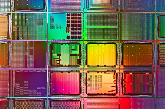
EUVL is a semiconductor manufacturing technology that uses 13.5 nm wavelength light to create small features on integrated circuits. The light is generated by a plasma source, often involving a laser hitting a tin droplet. Unlike traditional optics, EUVL relies on multilayer reflective mirrors to focus the EUV light onto the wafer. A mask, similar to a stencil but acting in reflection, defines the patterns to be transferred, with the photoresist on the wafer reacting to the light exposure. After development, the photoresist pattern is used as a mask for etching the underlying semiconductor layers. EUVL enables smaller features, higher resolution, and continued miniaturization of semiconductor components.
In 1997, Sandia joined forces with Lawrence Livermore and Lawrence Berkeley National Laboratories to create the Virtual National Laboratory, a groundbreaking consortium of national laboratories and industry – their research focused on EUVL and leveraged key capabilities from each Lab.
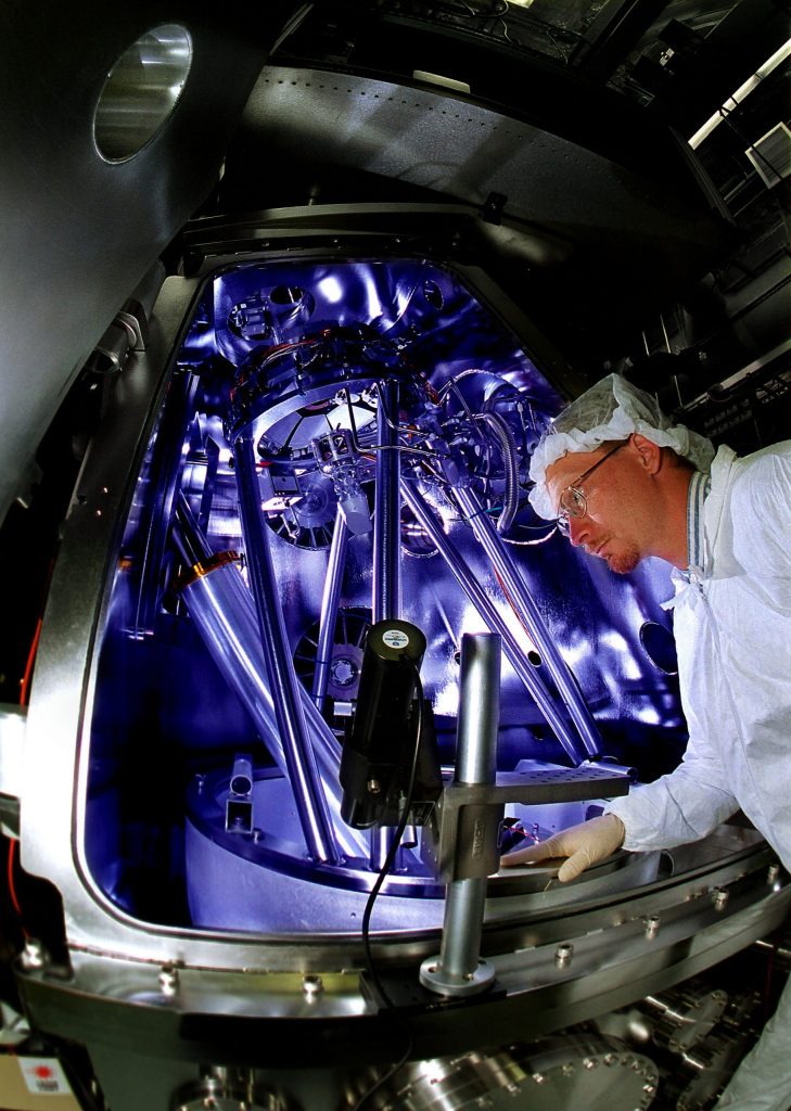
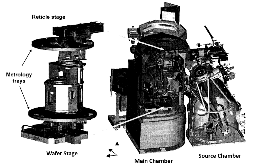
Within four years, the team developed the world’s first EUVL exposure machine, weighing 10 tons and measuring 10 feet tall. This tool, comprised of a main chamber alongside an illuminator, was capable of producing an image using 13.4 nanometer light from a laser plasma source. It was a tremendous leap forward in resolution. With this achievement, the team enabled the creation of much more powerful and energy-efficient chips with smaller transistors.
The foundational EUVL technology created by the consortium is the basis for EUVL today, though all manufacturing and iterative versions have been managed by industry since 2013. Nonetheless, without EUVL, commercial microchips and the recent advancement in artificial intelligence would be impossible. It remains the only method of making chips for the 3-5 nm technology node. The team forever left an impression on technological history, but perhaps more enthralling, is the impression the EUVL team left on each other decades ago. In the process of navigating a technical unknown, they overcame hurdles, created lasting bonds, and developed a building block of our modern world.
Dark-horse technology and people-first leadership
“It’s an amazing story in so many ways because of the people. It was the highlight of my career,” explained Rick Stulen with a smile.
Stulen was, and is, the cornerstone of the EUVL team. He joined Sandia’s hydrogen storage program in 1976 and became manager of Sandia’s surface science and chemical physics department in 1984. In the early 1990s, he developed one of Sandia’s largest Cooperative Research and Development Agreements (CRADA) to date, in partnership with Lawrence Livermore and Lawrence Berkeley, to form the $300 million EUVL program, funded by industry. Eventually, he became the Chief Operating Officer of the EUVL Virtual National Laboratory.
“I am driven by curiosity and a strong desire to be innovating—to always be thinking about new stuff. I’m not a solo guy. I think about what’s important for society—contributing to the big picture—and working with others to contribute,” said Stulen.
The project was initially funded by the domestic technology transfer initiative, funded by Congress in 1987. This funding allowed the three national laboratories to work with various commercial partners. Initial discussions quickly highlighted the need for a partnership that addressed a critical gap between semiconductor manufacturing capabilities and the growing need for advanced technologies.
“Sematech was so effective. Once a year everyone would get together and evolve the technical roadmap for chip manufacturing. EUVL was one lithography option, but we also discussed x-ray lithography, electron-based lithography and other things—all of which are different ways to make small features. At the end of one of the early Sematech meetings, attendees took a vote on the best option and EUVL came in dead last. But it didn’t deter us,” explained Stulen.
During this time, Sematech was created as a national consortium to lay out the roadmap for tech development needed in semiconductor manufacturing, from lithography to packaging.
Despite being voted as the least viable technological option to solve the manufacturing dilemma, Stulen and his peers dove in headfirst.
“I am an optimist. I knew EUVL was the dark horse, but we created this great lab network. So, I proposed the Virtual National Laboratory. All three labs—Sandia, Lawrence Livermore, and Lawrence Berkeley—came together under the same governance, rules, and business structure. It was unheard of at the time and a successful business structure, mainly due to the support of our leaders. We created a culture of equality—everyone was treated the same—regardless of what lab you worked for or what your title was,” said Stulen.
Over time, the Virtual National Laboratory created its own culture, combining fundamental science and state-of-the-art engineering, rooted in clear mission, innovation, and comradery. Two years after EUVL technology was downvoted as a dead-end option, the team was voted as the most probable solution to the growing semiconductor manufacturing issue.
Daunting problems
Sandia was responsible for designing and assembling the prototype EUV exposure tool called the Engineering Test Stand (ETS). Sandia also worked to solve technical challenges with the laser-produced plasma light source, the photoresist that captures the mask image carried by the EUV light, and the “environment” of the tool in which contamination issues can arise because EUV light is so energetic (short wavelength) that it can break chemical bonds. Lawrence Livermore provided expertise in mask and optics coating and testing, and Lawrence Berkeley focused on performance measurements at wavelength.


Lennie Klebanoff, previously a tenured Full Professor of Chemistry at Lehigh University, was hired by Rick in 1997 to serve as the EUVL Environment Team Lead. Klebanoff and his team of seven Sandians were tasked with reducing EUV-induced contamination of optic surfaces as well as particle contamination of the mask. In addition to reducing environmental contamination, Lennie’s team determined the materials that would be used to construct the ETS to minimize contamination problems.
“The contamination control that this technology requires is frightening,” Klebanoff recalls. “We needed to limit contamination of the optics to no more than several atomic layers. Also, the mask had to be protected from particle contamination which would spoil the transfer of the mask image. It was the equivalent of not allowing anything larger than a basketball over an area the size of the continental United States.”
Lennie remembers the first few months on the project as a mix of nerves and tackling the unknown, but the innovation that resulted and working with so many talented people at the labs and in industry was life-altering.
“We had whole teams dedicated to the issues that could occur during EUV chip manufacturing, and it was just so different than academia. I really enjoyed working with so many people. But the environmental problems scared me. I was pretty uptight about it. Fortunately, one day I confessed my fears to Stulen. His wonderful encouragement dissolved my fears, completely freed me up, and the answers started coming. Stulen gave everybody the confidence we needed to work on these hard problems, shared Klebanoff. “It was very gratifying work, and I’m so happy the work was useful and has had such an impact.”
“It was the equivalent of not allowing anything larger than a basketball over an area the size of the continental United States.”
Lennie Klebanoff, EUVL team lead speaking about the strict limitations on contamination in the technology
A technical legacy
Since the Virtual National Laboratory pioneered the foundation for modern-day EUVL technology, the impact has been hailed as the savior of Moore’s Law, which is the concept that the number of transistors on a circuit must double every two years to keep up with technological demands. Others say EUVL singlehandedly made artificial intelligence and robotics possible by enabling smaller transistors. EUVL, and the team behind the technology, significantly impacted current day capabilities, and while many on the team are proud of that accomplishment, it’s the teamwork and comradery they cherish most.
“I have such warm nostalgic feelings of friendship when I think about my fellow EUVL Sandians, our friends at LLNL and LBNL, and our industry partners too. It was such difficult work, but Rick Stulen created a true family environment which made it all happen,” shared Klebanoff.
Kurt Berger, who worked on the EUVL team as the Source Development Engineer and Sensor Engineer has a similar nostalgic perspective.
“I liked working for 12-15 hours straight and not realizing where the time went. The people were great, and everyone was focused on the same goal— to make the future better,” said Berger.
Along with creating a familial bond across various Laboratories, the team singlehandedly impacted modern technology and directly impacted Sandia’s history.
Sarah Allendorf, Director of Sandia’s Transportation and Industrial Processes programs, remembers the EUVL team as one of the most impactful in Sandia’s history, and one whose impacts are still felt today.
“I love many things about EUVL. Technically, it started from people thinking really big—they had a crazy idea to create a light source that had to be robust and consistent. It was a crazy vision at the time. Logistically, it was a huge CRADA, and to get all of the institutions to agree was a monumental task,” explained Allendorf. “It’s so much more than just the technology—it was state-of-the-art physics and business and clever work that we still apply to many problems.”
Together, the team went against the grain to create new ways of working and new ways of innovating. They pulled expertise from across laboratories, partnered with industry, and fostered a safe environment to try new things without fear of failure.
“Nothing was impossible at that time,” shared Stulen. “Our purpose was always clear, and we were energized by the need to solve an issue. But what was so motivating is that everyone was involved – like cousins from different countries all sitting at the same dinner table. Together, we accomplished our goal to demonstrate the feasibility of this technology and it’s because everyone had a piece of the puzzle—we just needed to put it together.”
April 7, 2026