Campus-like facilities integrate nuclear weapons design and microsystems manufacturing
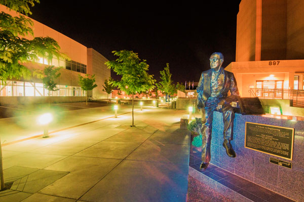
The buildings and structures at Sandia reflect a rich and varied 70-year architectural history. This is the third in a series of articles that explore the built environment of the Labs and the people who laid its foundation. See also Building Sandia: 1940s to 1960s and Building Sandia: Late 1960s to mid-1990s.
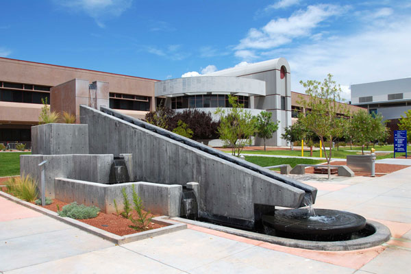
Sandia’s Microsystems and Engineering Sciences Applications Complex is set apart aesthetically and functionally from other buildings and sites at the Labs. The complex is characterized by open spaces, community areas, pedestrian walkways and a unique water feature, elements that are intended to emphasize the integration of nuclear weapons design and microsystems manufacturing.
This intentional campus-like design connects 1980s-era facilities with newer, greener building construction. As the complex has taken shape over the decades, its architecture has maintained the same state-of-the-art quality as the facility’s microelectronics capability that has influenced nearly every mission area at Sandia.
The idea for MESA facilities has its origins in the 1970s, when weapons designers at Sandia recognized the potential for large-scale integrated circuits to combine increased complexity with higher reliability — all in a smaller, lighter package. However, nuclear weapons design required that the components also be radiation-hardened and produced in relatively small lots.
This was difficult to come by in commercial production, so the Labs pursued in-house capabilities and, by 1975, was delivering custom, radiation-hardened microelectronics. The development of many satellite and space applications, such as the NASA Galileo space probe, were facilitated by Sandia’s advances in this area.
This early pioneering work was performed in various buildings and small laboratories across the site. The Semiconductor Development Laboratory in Tech Area 1 housed cleanroom technology enabled by Willis Whitfield’s 1960 laminar flow cleanroom design (the building has since been extensively renovated and is now home to neutron generator production). Also, as a result of this early work, the Radiation-Hardened Integrated Circuits process and components were adopted more broadly by the semiconductor industry.
CSRL and MDL
In 1987, Sandia added the Compound Semi-conductor Research Lab, which included a Class 100 cleanroom space and was used for early device research based on strained layer superlattice research pioneered at Sandia. Designed with a five-year life expectancy, CSRL operated for 20 years, until its research was absorbed into the MESA Complex.
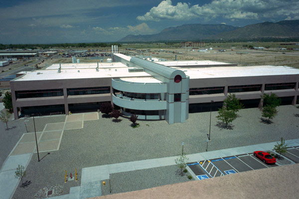
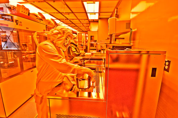
In 1988, the Microelectronics Development Laboratory was built to support Sandia’s primary research role for strategic radiation-hardened, silicon-based microelectronics and manufacturing efforts. It was the most advanced, flexible and responsive facility for microelectronics research at that time. The MDL was the first purpose-built facility constructed specifically for silicon microelectronics mission work, its configuration accommodating a Class 1 cleanroom. Jack DeBartolo Jr. of Tucson, Arizona, a specialist in high-tech facility design, served as lead architect.
The three-story MDL building is steel framed with a substantial pedestal foundation to manage manufacturing equipment weights and vibration sensitivity. From an aerial perspective, the MDL site looks like an integrated circuit — the “pins” are the air circulation elements of the cleanrooms, which change the air five to six times per minute in the constant airflow of the cleanrooms.
Breaking new ground
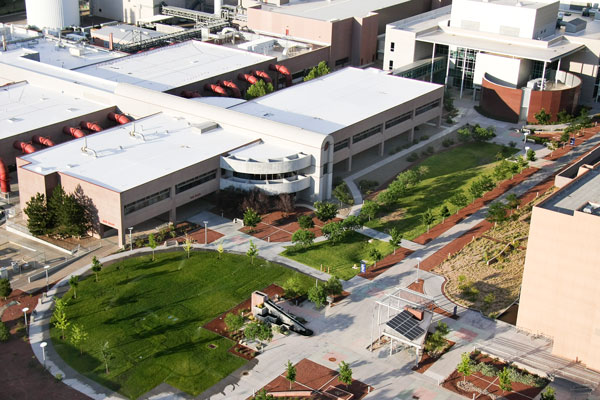
In August 2003, Sandia broke ground on the new MESA Complex to expand, enhance and combine its microelectronics work. The MESA Complex construction effort was completed in 2007, with the addition of the MicroFab and the MicroLab, along with the Weapons Integration Facility. This multi-phase construction project was led by architects from Carter Burgess, a Dallas firm. A feature of the architectural design is the polished stone and steel curvilinear walls that lead to the main entrances of the buildings. Wings off the buildings are accented by ribbons of windows with unique, louvered sunshades.
Like the MDL, the MicroFab building is a three-story microsystems design, development and production facility with a state-of-the-art Class 10 cleanroom. This facility has a more modern configuration that provides flexibility in the types of materials and applications used for research, facilitating the ability to develop microsystems such as micromechanical devices and photonics technologies that Sandia pioneered both here and at the Center for Integrated Nanotechnologies.
The 400,000-square-foot MESA Complex stands as the largest capital project at Sandia funded by Congress, as well as Sandia’s largest construction project since the first permanent buildings were constructed in the 1940s. Other features of the project are the shared utilities with other production facilities.
Construction of the MESA Complex was completed ahead of schedule and under budget, earning kudos from DOE. Sandia was permitted to reinvest unused funds from the project into the development of its new Ion Beam Lab.
The MESA Complex represents a crucial crossroad in the history of Sandia’s architecture: a time when building aesthetics and innovations fully combined with functionality.
Related: MESA fabs get an upgrade
