LDRD Grand Challenge project could transform electronics, solve energy challenges
Like so many projects before it, this one started with some good questions. Arguably, too many.
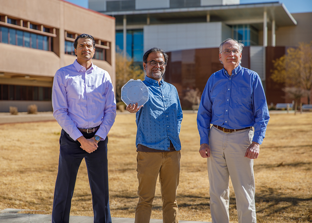
The first question seemed simple enough: Could certain specialized fabrication techniques impact fields outside of quantum information science? But as soon as Sandia physicist Shashank Misra started to unpack it, he discovered a monster of a problem that was difficult to solve with a conventional research project.
“There were so many interwoven science questions that any regular Laboratory Directed Research and Development project might answer one or a few but wouldn’t reduce the overall risk because there wouldn’t be time to address the others,” Shashank said.
His idea was to take qubit fabrication methods originally developed by researchers in Australia, and later adopted by Sandia, for quantum computing and use these methods to make microelectronics.
The payoff could be huge — a fundamentally new way to build integrated circuits, power electronics and other semiconductor devices. New quantum microelectronics could potentially be as transformative as quantum computers and quantum sensors, and they could be a key to solving looming energy challenges.
“The power demand for electronics is going to outstrip the world’s capability for generating power, based on current trends,” said Paul Sharps, manager over Sandia advanced electronic and optoelectronic materials. “I think it’s very critical that we invest now in other sorts of electronic devices that significantly reduce power consumption.”
A Grand Challenge emerges
The toolkit Shashank wanted to use is called atomic precision advanced manufacturing, which he and others simply call APAM. It’s a collective term for technologies that let researchers control where individual atoms go in a device.
“The transistors involved in microelectronics for the last 40 years have used one form of physics,” said Conrad James, one of the Grand Challenge’s strategists and a former Grand Challenge principal investigator in his own right. “What APAM does is open up different physics to perform the switching in microelectronics, and that provides a wide range of opportunities for improvements in microelectronics, including reduced power consumption and new types of sensors.”
But Shashank said there were too many open questions to get the idea off the ground. Nobody was willing to fund their project ideas.
“The place where we ran into it headlong was when we would pitch application ideas where having atomic-scale control was really important. The push back was there were too many open science questions that could prevent having a significant impact. It was either that, or if we were to show in principle that having atomic-scale control opens up this opportunity space, there is no path to implement it in a way that works alongside current technologies. Up to that time nobody had shown that devices could work outside of a cryostat,” a machine that maintains ultra-low temperatures, Shashank said.
So, he changed his tack. Instead of jumping to applications, he decided to tackle some of the open science questions by pulling together a cross-disciplinary team — an approach perfectly suited for a Grand Challenge LDRD.
The FAIR DEAL Grand Challenge, short for Far-reaching Application, Implication and Realization of Digital Electronics at the Atomic Limit, ran from fiscal years 2019 through 2021.
With a team of 36 people over three years, Shashank aimed to answer three main questions: Can Sandia-developed atomic precision advanced manufacturing build a device that is compatible with CMOS, the industry-standard method of semiconductor manufacturing? Can it be accomplished in a practical environment (i.e., not at cryogenic temperatures)? Does the final product do anything special that a conventional device can’t?
Shashank never expected the answers would be yes, yes and yes.
“If somehow I had a genie grant me a wish at the beginning of the project, the truth is I would have wished for less,” he said.
“In any project this ambitious, you think about it in terms of triage,” he said. “What’s the off-ramp when A works, and B doesn’t work? What’s the off-ramp when it’s vice versa? I think the most surprising thing was, in general, there may be a lot of engineering difficulty, but there is no basic obstacle holding you back. The fact that all of those things were true was very surprising to me.”
Creating new engineering opportunities
The FAIR DEAL team successfully built a microchip in which an APAM nanodevice worked directly in concert with a CMOS circuit built at the Microsystems Engineering, Science and Applications Complex. Not only did the combined circuit work as planned, and at room temperature, but the team also demonstrated that APAM devices shouldn’t compromise the robustness of the microchip.
As FAIR DEAL began answering scientific questions, Shashank and his team were able to restart conversations about applying the manufacturing methods to specific uses. In 2021, a spin-off project began with DOE’s Advanced Manufacturing Office, aiming at developing what FAIR DEAL began for energy-efficient microelectronics.
Paul, who was a member of the Grand Challenge, said, “I saw that as a major step forward because I saw that as being recognition from an outside agency, not just Sandia, that’s willing to put money into something — that this is really key, that this is really a breakthrough. All the parts need to get put together, but enough things have been done to really tee that up for outside recognition and funding.”
Sandia has also begun several collaborations with university partners, and the team is in talks with potential sponsors about whether this new way of processing silicon could create opportunities to implement new kinds of hardware trust and security measures.
Shashank says that his team’s success has opened even more scientific questions that need to be studied.
“We have atomic-scale control over some elements in silicon,” he said. “And I think the science opportunities that other people are pursuing on the project at this point are looking at whether we can have atomic-scale control in every material. There’s a lot of thought that has to go into how you do that, but I do think that’s where the science is headed.”