After 60 years of producing continuously smaller electronic devices, the silicon semiconductor industry now sits firmly in the realm of nanoscale dimensions. Gate lengths smaller than 20 nanometers are common in modern silicon-based transistors. Meanwhile, research involving novel materials and 2D materials with exotic properties points to alternatives to silicon for the next-generation electronics. Among the challenges in developing such devices is the task of accurately predicting the behavior of a proposed design.
For decades, microelectronic devices such as metal-oxide-semiconductor field-effect transistors, also called MOSFETs, have been modeled using semi-classical approaches — by solving the drift-diffusion equations for electrons and holes, while incorporating quantum-mechanical effects through phenomenological models calibrated with parameters fitted to experimental data. This methodology, implemented in various commercial technology computer-aided design device software, has played a critical role in advancing microelectronics to its current state. Sandia also developed its own technology computer-aided design platform, Charon, to support mission-driven device simulation needs.
However, as devices continue to shrink or are made from emerging materials, the long relied-upon modeling methodology is approaching its limits. At these limits, the techniques involved fail to capture the true behavior of nanoscale devices, which are dictated largely by quantum-mechanical effects. Most importantly, these techniques lack predictive accuracy.
To address this anticipated limitation, a team of experts from Sandia’s Cognitive & Emerging Computing organization has developed a predictive quantum transport simulation framework. This software, called CBR3D, is designed to predict and simulate the behavior of nanodevices with a minimum of fitting parameters and with great accuracy. This tool has demonstrated strong predictive capabilities, enabling advancement in both today’s state-of-the-art as well as emerging technologies that exceed the limitations of current complementary metal oxide semiconductor technologies.
In addition, and unlike commercial alternatives, CBR3D can model devices with arbitrary geometries and multiple current-carrying contacts. The simulator includes the relevant forms of both elastic and inelastic scatterings, including electron-electron interaction, electron-phonon interaction, and scattering from discrete charged impurities.
Accurate prediction relies in part on understanding with great specificity how the device’s state will change during operation when differences in voltage are applied across its contacts. The team’s model-building framework includes a rigorous, first-principles approach that examines behavior of charges through the device. This approach relies on a mathematical formalism known as the non-equilibrium Green’s function, which solves the Schrödinger equation under non-equilibrium conditions.
Through several Laboratory Directed Research and Development projects, the Sandia team has demonstrated the accuracy and predictive power of its first principles-based simulation framework for modeling both state-of-the-art and beyond-CMOS devices. Leveraging Sandia’s high-performance computing resources has been essential for efficiently overcoming the significant computational challenges inherent in these demanding simulations and for advancing the technology.
State-of-the-art CMOS devices
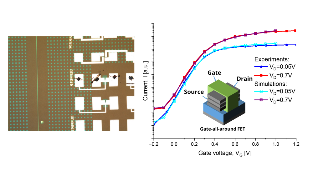
Gate-all-around field-effect transistors represent the next-generation device architecture being widely adopted by the semiconductor industry to enable continued downscaling beyond the 3-nm technology node and to surpass the capability of fin field-effect transistors, which are the most advanced transistor technology used today.
This shift will come with two major changes to GAAFETs: (1) For the first time in commercially available CMOS technology, GAAFETs channels and potentially source and drain are fully insulated from the substrate by a dielectric layer, offering complete insulation; and (2) integration of Silicon-Germanium into the device channel to enhance hole mobility. These novel features may enhance their potential hardening to certain types of radiation exposure, making them particularly attractive to Sandia for use in computing systems across a range of mission-critical applications. Through a partnership with IBM, and leveraging the CBR3D code, the Sandia team has successfully simulated IBM’s GAAFET device and accurately reproduced the measured electrical response, as illustrated in Figure 1, demonstrating the high fidelity in modeling state-of-the-art CMOS devices.
The team has also used this framework to uncover new physical phenomena in GAAFETs. For instance, it has helped explain the observed increase in leakage current in the deep subthreshold regime and has suggested mitigation strategies to support the design of future high-performance, agile, and resilient systems for national security applications. Furthermore, ongoing efforts are now focused on investigating the effects of radiation on the performance of GAAFETs. These studies aim to identify the dominant defect mechanisms and quantify their impact on circuit degradation, ultimately guiding the development of more robust electronics for extreme environments.
Beyond-CMOS devices
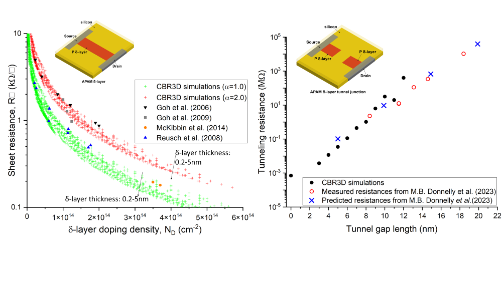
Recent advancements in Atomic Precision Advanced Manufacturing at Sandia have opened new avenues for fabricating novel devices based on quasi-2D, highly doped regions — known as δ-layers — in a semiconductor material. These innovations are paving the way for beyond-CMOS technologies that support the development of the next-generation classical and quantum computing applications.
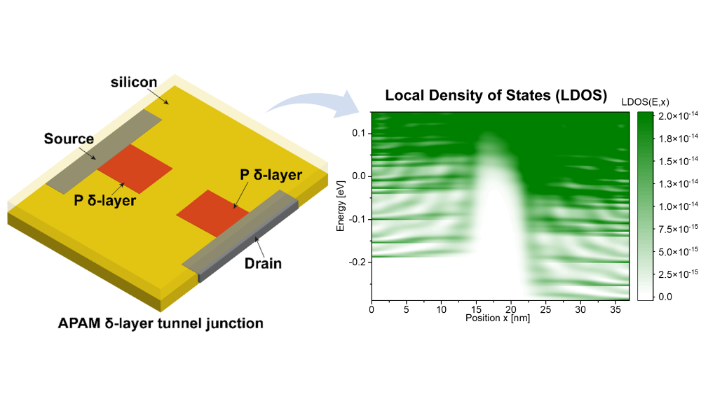
The Sandia team has employed the advanced computational capability to investigate these emerging systems. Their simulations have accurately predicted the electronic properties observed experimentally, as illustrated in Figure 2, highlighting the predictive power of the modeling framework for beyond-CMOS devices. Furthermore, the simulations have uncovered previously unobserved quantum-mechanical phenomena in these systems (Figure 3), leading to the identification of novel applications for APAM-enabled devices, such as charge sensing, and resulting in multiple patent applications.
Looking at the future
The rapid rise of AI applications has significantly increased the energy consumption in computing—especially in data centers. In response, several U.S. agencies are leading efforts to reduce the computational energy demands by developing novel, high energy-efficiency computing architectures. Achieving this national goal will require predictive device simulations, enabled by our developed computational framework, to guide the design and development of the necessary technologies.