30 years ago Sandia led the development of a foundational technology
Microchips are a cornerstone of daily life. Nearly every device we rely on includes a tiny microchip and its even smaller circuits.
However, despite our reliance on the technology, few know how a team of Sandians in California and New Mexico and their partners at Lawrence Livermore and Lawrence Berkeley national laboratories contributed to the foundation of microchip development and, in the process, created a bond spanning decades.
New era, new demands
As technology and tools advanced in the 1990s, pressure grew to create higher performing microchips to accommodate growing needs and capabilities. No one could identify a cost-effective, accurate way to create higher performing chips that required higher chip density and smaller features, which required shorter wavelengths of light to etch the details. A team of researchers at Sandia believed an emerging technology, called extreme ultraviolet lithography, or EUVL, potentially held the key to shorter wavelengths and higher chip density.
In 1997, Sandia joined forces with Lawrence Livermore and Lawrence Berkeley to create the Virtual National Laboratory, a groundbreaking consortium of national laboratories and industry. Their research focused on EUVL and relied on key capabilities from each lab.
“It’s an amazing story in so many ways because of the people. It was the highlight of my career,” Sandia retiree Rick Stulen said.
Stulen was, and is, the cornerstone of the EUVL team. He developed one of Sandia’s largest Cooperative Research and Development Agreements to date, in partnership with Lawrence Livermore and Lawrence Berkeley, to form the $300 million EUVL program, funded by Intel, IBM, AMD, Motorola and others. Eventually, he became the chief operating officer of the EUVL Virtual National Laboratory.
“I am driven by curiosity and a strong desire to be innovating — to always be thinking about new stuff,” Stulen said. “I’m not a solo guy. I think about what’s important for society, contributing to the big picture and working with others to contribute.”
Intersection of industry and imagination
During this time, Sematech was created as a national consortium to lay out the roadmap for tech development needed in semiconductor manufacturing, from lithography to packaging.
“Sematech was so effective,” Stulen said. “Once a year, everyone would get together and evolve the technical roadmap for chip manufacturing. EUVL was one lithography option, but we also discussed X-ray lithography, electron-based lithography and other things — all of which are different ways to make small features. At the end of one of the early Sematech meetings, attendees took a vote on the best option and EUVL came in dead last. But it didn’t deter us.”
Despite being voted as the least viable technological option to solve the manufacturing dilemma, Stulen and his peers persisted.
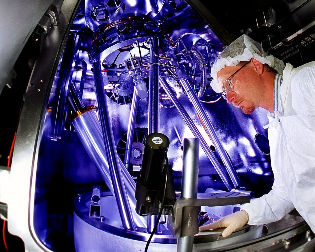
Within four years, the team developed the world’s first EUVL exposure machine, weighing 10 tons and measuring 10 feet tall. This tool, composed of a main chamber alongside an illuminator, could produce an image using 13.4-nanometer light from a laser plasma source. It was a tremendous leap forward in resolution, enabling much more powerful and energy-efficient chips with smaller transistors that are made today with modern EUVL.
“I am an optimist,” Stulen said. “I knew EUVL was the dark horse, but we created this great lab network, the Virtual National Laboratory. It was unheard of at the time and a successful business structure, mainly due to the support of our leaders. We created a culture of equality — everyone was treated the same — regardless of what lab you worked for or what your title was.”
One way forward
Two years after EUVL technology was downvoted as a dead-end option, it was voted as the most probable solution to the growing semiconductor manufacturing issue.
Sandia was responsible for designing and assembling the prototype extreme ultraviolet lithography exposure tool called the Engineering Test Stand. Sandia also worked to solve technical challenges inherent in such bleeding-edge technology.
Stulen hired Lennie Klebanoff in 1997 to serve as the EUVL environment team lead. Lennie and his team of seven Sandians were tasked with reducing extreme ultraviolet lithography-induced contamination of optic surfaces as well as particle contamination of the mask.
“The contamination control that this technology requires is frightening,” Lennie said. “We needed to limit contamination of the optics to no more than several atomic layers. Also, the mask had to be protected from particle contamination, which would spoil the transfer of the mask image. It was the equivalent of not allowing anything larger than a basketball over an area the size of the continental United States.”
Lennie remembers the first few months on the project as a mix of nerves and tackling the unknown, but the innovation that resulted and working with so many talented people at the laboratories and in industry was life-altering.
“I really enjoyed working with so many people,” Lennie said. “But the environmental problems scared me. I was pretty uptight about it. Fortunately, one day I confessed my fears to Rick. His wonderful encouragement dissolved my fears, completely freed me up, and the answers started coming. It was very gratifying work, and I’m so happy the work was useful and has had such an impact. “
Kurt Berger, who worked on the EUVL team as the source development engineer and sensor engineer, has a similar nostalgic perspective.
“I liked working for 12-15 hours straight and not realizing where the time went,” Kurt said. “The people were great, and everyone was focused on the same goal: to make the future better.”
Sarah Allendorf, director of Sandia’s Transportation and Industrial Processes programs, remembers the EUVL team as one of the most impactful in Sandia’s history, and one whose impacts are still felt today.
“I love many things about EUVL,” Sarah said. “Technically, it started from people thinking really big. Logistically, it was a huge CRADA, and to get all of the institutions to agree was a monumental task. It’s so much more than just the technology — it was
state-of-the-art physics and business and clever work that we still apply to many problems.”
A better future
Since the Virtual National Laboratory pioneered the foundation for modern-day EUVL technology, the impact has been hailed as the savior of Moore’s Law, which is the concept that the number of transistors on a circuit must double every two years to keep up with technological demands. Others say EUVL singlehandedly made artificial intelligence and robotics possible by enabling smaller transistors. While many on the team are proud of that accomplishment, it’s the teamwork and comradery they cherish most.
“I have such warm nostalgic feelings of friendship when I think about my fellow EUVL Sandians, our friends at Lawrence Livermore and Lawrence Berkeley, and our industry partners too,” Lennie said. “It was such difficult work, but Rick created a true family environment, which made it all happen.”
“Nothing was impossible at that time,” Stulen said. “Our purpose was always clear, and we were energized by the need to solve an issue. But what was so motivating is that everyone was involved — like cousins from different countries all sitting at the same dinner table. Together we accomplished our goal to demonstrate the feasibility of this technology, and it’s because everyone had a piece of the puzzle. We just needed to put it together.”