
A deep understanding of the properties and underlying physics of materials is critical to the success of quantum information science and technology. Over the past 20 years Sandia has been pursuing research that both help us understand materials that enable quantum systems, as well as quantum materials that can be devices themselves.
Expand the sections below for information on the key capabilities and featured projects in each of these areas that our program is currently pursuing:
Quantum materials are materials that exhibit novel physical properties that can potentially be leveraged for next-generation computing and sensing with groundbreaking performance. The Sandia team specializes in nanoscale fabrication, integration, and electrical and optical characterization, with a goal of understanding the electronic structure of the material and their implications in electrical and optical properties.
Key Capabilities
We have fabrication and integration capabilities for creating nanoscale quantum structures, such as tunnel junctions, superconductor-semiconductor interfaces, quantum point contacts and quantum dots, for studying mesoscopic quantum physics enabled by quantum materials. We also have structural electrical, and optical characterization capabilities, such as scanning probe microscopy, electron microscopy, Raman spectroscopy, microwave spectroscopy, magneto-transport, for resolving the nanoscale structures spatially and spectroscopically.
Featured Projects
Group IV heterostructures for quantum physics and engineering:
- A. J. Miller, M. Brickson, W. J. Hardy, C.-Y. Liu, J.-Y. Li, A. Baczewski, M. P. Lilly, T. M. Lu, D. R. Luhman, “Effective out-of-plane g-factor in strained-Ge/SiGe quantum dots,” Phys. Rev. B, 106, L121402 (2022).
- C.-T. Tai, P.-Y. Chiu, C.-Y. Liu, H.-S. Kao, C. T. Harris, T. M. Lu, C.-T. Hsieh, S.-W. Chang, and J.-Y. Li, “Strain Effects on Rashba Spin-Orbit Coupling of Two-dimensional Hole Gases in GeSn/Ge Heterostructures,” Adv. Mater., 33, 2007862 (2021).
- C.-T. Chou, N. T. Jacobson, J. E. Moussa, A. D. Baczewski, Y. Chuang, C.-Y. Liu, J.-Y. Li, and T. M. Lu, “Weak anti-localization of two-dimensional holes in germanium beyond the diffusive regime,” Nanoscale 10, 20559 (2018). (Cover)
- L. N. Maurer, J. K. Gamble, L. Tracy, S. Eley, and T. M. Lu, “Designing nanomagnet arrays for topological nanowires in silicon,” Phys. Rev. Appl. 10, 054071 (2018).
- T. M. Lu, L. A. Tracy, D. Laroche, S.-H. Huang, Y. Chuang, Y.-H. Su, J.-Y. Li, and C. W. Liu, “Density-controlled quantum Hall ferromagnetic transition in a two-dimensional hole system,” Sci. Rep. 7, 2468 (2017).
Superconducting proximity effect:
- M. Hatefipour, J. J. Cuozzo, J. Kanter, W. Strickland, T. M. Lu, E. Rossi, and J. Shabani, “Induced superconducting pairing in integer quantum Hall edge modes of InAs,” Nano Lett., 15, 6173 (2022).
High-kinetic inductance superconducting devices:
- T. M. Bretz-Sullivan, R. M. Lewis, A. L. Lima-Sharma, D. Lidsky, C. Smyth, C. T. Harris, M. Venuti, S. Eley, and T. M. Lu, “High kinetic inductance NbTiN superconducting transmission line resonators in the very thin film limit,” Appl. Phys. Lett., 121, 052602 (2022).
In the past few decades, it has become increasingly recognized that quantum and strong electron-correlation effects at the nano and microscale can fundamentally modify, in rich and novel ways, materials properties at the macroscale.
This has led to the naming of an entirely new class of materials – quantum materials. Topological quantum materials are a recent example – one which could be of great significance for quantum information science, since they hold the promise of robustness against the decoherence that is ubiquitous in current qubit implementations in quantum computation. At Sandia, we further aim to explore artificial quantum materials, artificial materials designed and constructed from existing materials through sophisticated nanofabrication and intended specifically to produce and study unique quantum phenomena for quantum information science.
Key Capabilities
We have developed extensive experience in the growth of high quality single crystals and compound semiconductor materials.
We have access to a suite of sophisticated state-of-the-art nanofabrication techniques, including electron-beam lithography (EBL), interferometric lithography (IL), nanoimprint and photolithography for nano/micro scale device fabrications and for creating artificial quantum materials.
We have developed a suite of sophisticated theoretical tools for quantum materials and artificial quantum materials, including the density functional theory, tight-binding calculations, effective-mass theory, etc.
We have built multiple cryogenic systems dedicated to quantum transport measurements of both static and dynamic properties of the quantum states realized in quantum materials and artificial quantum materials. Extensive high frequency filtering stages are installed in these cryogenic systems so that they are suitable for low noise and high precision ultra-low temperature studies of superconductivity and exciton condensation.
Featured Projects
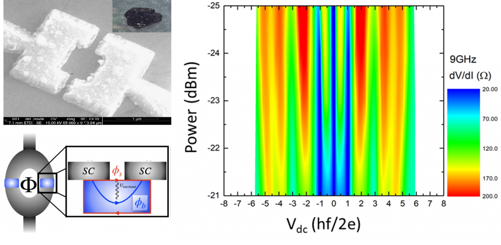
Novel Josephson effects in topological Dirac semimetals
It has been suggested that topological superconductivity can be achieved in nontrivial surface states of topological quantum materials, for example Dirca semimetals, by utilizing the superconductor proximity effect. At Sandia, we have made exciting discoveries of novel Josephson effects in topological Josephson junctions (JJs) and superconducting quantum interference devices (SQUIDs) in Cd3As2, an exemplar Dirac semimetal. Both π and 4π periodic supercurrents in aluminum-Cd3As2-aluminum JJs are observed. Our data analysis suggests that the π period arises from interference between the induced bulk superconductivity and the induced Fermi-arc surface superconductivity, while the 4π period is manifested by the missing first Shapiro steps and is expected for topological superconductivity. Moreover, our study of ac Josephson effects in Cd3As2 topological SQUIDs leads to a surprising discovery of the Leggett modes, a collective quantum phenomenon predicted more than 50 years ago.
- J.J. Cuozzo, W. Yu, P. Davids, T.M. Nenoff, D.B. Soh, W. Pan, and E. Rossi, Leggett Modes in Dirac Semimetals, https://arxiv.org/abs/2205.15995 (2022).
- Eric Chatterjee, Wei Pan, and Daniel Soh, Microwave photon number resolving detector using the topological surface state of superconducting cadmium arsenide, Phys. Rev. Research 3, 022036 (2021).
- W. Yu, Rafael Haenel, M. A. Rodriguez, S. R. Lee, F. Zhang, M. Franz, D. I. Pikulin, and W. Pan, Zero-bias conductance peak in Dirac semimetal-superconductor devices, Phys. Rev. Research 2, 032002(R) (2020).
- S.R. Lee, P.A. Sharma, A.L. Lima-Sharma, W. Pan, and T.M. Nenoff, Topological quantum materials for realizing Majorana quasiparticles, Chemistry of Materials 31, 26 (2019).
- W. Yu, W. Pan, D. L. Medlin, M. A. Rodriguez, S. R. Lee, Z.-Q. Bao, and F. Zhang, π and 4π Josephson Effects Mediated by a Dirac Semimetal, Phys. Rev. Lett. 120, 177704 (2018).
Semiconductor twistronics
Here, we aim to advance the field of artificial quantum materials for quantum information science applications by exploring strong electron correlation physics and topological phenomena in artificial graphene and moiré superlattices composed entirely of conventional compound semiconductor heterostructures. The overarching thesis/hypothesis of this research is that semiconductor-based artificial quantum materials will enable the tunability of three fundamental parameters associated with quantum materials: electron-electron interactions, spin-orbit coupling, and band topology. Such tunability will both help unravel quantum-materials phenomena that have already been observed but are yet poorly understood, as well as enable discovery of new quantum-materials phenomena that are not yet observed.
- W. Pan, J.L. Reno, D. Li, and S.R.J. Brueck, Quantum Hall Ferromagnetism in the Presence of Tunable Disorder, Phys. Rev. Lett. 106, 156806 (2011).
- S.K. Lyo and W. Pan, Nonlinear transport in a two-dimensional electron gas with a periodically modulated potential, Phys. Rev. B 84, 195320 (2011).
Fault tolerant qubits based on novel superconductor-InAs/GaSb semiconductor structures
Fault tolerance is currently the biggest obstacle toward the realization of a quantum computer. Advances in materials and device structures design are key to reduce the decoherence of the qubits states. Topological qubits, by using the so-called Majorana zero modes, are intrinsically protected from decoherence, and so offer a very attractive solution to a fault-tolerant quantum computer. The collaboration between Sandia and the College of William & Mary aims to combine materials advances and the topological approach to achieve high quality, InAs/GaSb semiconductor-based structures and Josephson junctions, to address the major hurdle on the path to a quantum computer. InAs/GaSb type-II heterostructures are grown via molecular beam epitaxy. High quality topological Josephson junctions are fabricated by e-beam lithography. These devices have the potential to support Majorana zero modes even when no magnetic field is present. This would be a significant achievement because it would allow a much greater freedom in the layout of networks of topological qubits. The outcomes of the proposed research will constitute a significant advance toward the realization of artificial quantum-coherent systems with new functionalities for quantum information science.
- D.P. Cummings, D.L. Perry, L.J. Jauregui, J. Deitz, J.F. Klem, W. Pan, and P. Lu, Observation of Focused Ion Beam-Induced Artifacts in Transmission Electron Microscopy Samples Leading to the Epitaxial Growth of AlGaSb Quantum Dots on the GaSb Substrate, Microscopy and Microanalysis 29, 138-144 (2023).
- K. Sun, Z.Q. Bao, W. Yu, S.D. Hawkins, J.F. Klem, W. Pan, and X. Shi, Charge transport spectra in superconductor-InAs/GaSb-superconductor heterostructures, Nanotechnology 33, 085703 (2022).
- W. Yu, V. Clericò, C. Hernández Fuentevilla, X. Shi, Y. Jiang, D. Saha, W.K. Lou, K. Chang, D.H. Huang, G. Gumbs, D. Smirnov, C.J. Stanton, Z. Jiang, V. Bellani, Y. Meziani, E. Diez, W. Pan, S.D. Hawkins, and J.F. Klem, Anomalously large resistance at the charge neutrality point in a zero-gap InAs/GaSb bilayer, New Journal of Physics 20, 053062 (2018).
- Y. Jiang, S. Thapa, G. D. Sanders, C. J. Stanton, Q. Zhang, J. Kono, W. K. Lou, K. Chang, S. D. Hawkins, J. F. Klem, W. Pan, D. Smirnov, and Z. Jiang, Probing the semiconductor to semimetal transition in InAs/GaSb double quantum wells by magneto-infrared spectroscopy, Phys. Rev. B 95, 045116 (2017).
- Jian Li, Wei Pan, Roman M. Lutchyn, and B. Andrei Bernevig, Detection of Majorana Kramers pairs using a quantum point contact, Phys. Rev. Lett. 117, 046804 (2016).
- G. C. Dyer, X. Shi, B. V. Olson, S. D. Hawkins, J. F. Klem, E. A. Shaner, and W. Pan, Far Infrared Edge Photoresponse and Persistent Edge Transport in an Inverted InAs/GaSb Heterostructure, Appl. Phys. Lett. 108, 013106 (2016).
Patents
| Title | Patent Number | Grant Date |
|---|---|---|
| Feedback-based quantum optimization | US12306900B1 | 05/20/2025 |
| Remote quantum state transfer for qubits with different frequencies | US11177890B1 | 11/16/2021 |
| Spin-orbit qubit using quantum dots | US10482388B1 | 11/19/2019 |
| Electron spin-based information shuttling for a computer system | US10002328B1 | 06/19/2018 |
| Semiconductor adiabatic qubits | US9530873B1 | 12/27/2016 |
| Isolating and moving single atoms using silicon nanocrystals | US7790051B1 | 09/07/2010 |