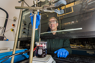
Graham Yelton and Sandia colleagues have developed a single electroforming technique that tailors key factors to better thermoelectric performance: crystal orientation, crystal size and alloy uniformity. The work is outlined a paper, “Using Galvanostatic Electroforming of Bi1-xSbx Nanowires to Control Composition, Crystallinity and Orientation,” in the Jan. 28 edition of the Materials Research Society’s MRS Bulletin. (Photo by Randy Montoya)
It’s all about efficiency in the small world of thermoelectric nanowires. Sandia researchers say better materials and manufacturing techniques for the nanowires could let carmakers harvest power from the wasted heat of exhaust systems or lead to more efficient devices to cool computer chips.
Researchers at Sandia’s campuses in New Mexico and California published a paper, “Using Galvanostatic Electroforming of Bi1-xSbx Nanowires to Control Composition, Crystallinity and Orientation,” in the Jan. 28 edition of the Materials Research Society’s MRS Bulletin. The authors are W. Graham Yelton, Steven J. Limmer, Douglas L. Medlin, Michael P. Siegal, Michelle Hekmaty, Jessica L. Lensch-Falk, Kristopher Erickson, and Jamin Pillars.
The work was the first time researchers managed to control crystal orientation, crystal size and alloy uniformity by a single process. All three factors contribute to better thermoelectric performance, Graham says.
“The three together mean a huge gain, and it’s hard to do,” he says. “It’s turning the knobs of the process to get these things to behave.”
Better nanowire geometries can reduce heat conductivity and improve what’s called the thermoelectric figure of merit, a measure of a material’s electrical and thermal conductivity. The higher the electrical conductivity and the lower the thermal conductivity, the higher the figure of merit and, therefore, the more efficient the material. However, the quality of thermoelectric nanowires in the past proved inadequate.
Thermoelectric nanowire use in its infancy
Despite their inefficiency, some thermoelectric materials are already in use. Graham compares their stage of development to the early days of solar photovoltaic cells: Everyone saw the potential, but they were so inefficient they were used only when nothing else worked.
Improved efficiency in nanowires would increase the use of thermoelectric materials. Graham says they’re already used in some sensors, and vehicle manufacturers are looking at their potential to harvest heat from exhaust systems to power vehicle sensor systems. Decreasing the power needed to run a vehicle’s operating system could reduce battery and alternator weight and perhaps eliminate some power-generating equipment, trimming vehicle size and weight.
Sandia’s paper describes how the team created thermoelectric nanowire arrays with uniform composition along the length of the nanowire and across the spread of the nanowire array, which potentially can include hundreds of millions of nanowires. In addition, they created nanowire crystals of uniform size and orientation, or direction. Uniform composition improves efficiency, while orientation is important so electrons, the carriers of energy, flow better.
The team used a cost-effective method called room-temperature electroforming, which is widespread in commercial electroplating. Electroforming deposits the material at a constant rate, which in turn allows nanowires to grow at a steady rate. The method produced wires 70-75 nanometers in diameter and many microns long.
Graham used pulses of controlled current to deposit the thermoelectric material to control composition throughout the wire and the array. “There are little nuances in the technique that I do to allow the orientation, the crystal growth, and the composition to be maintained within a fairly tight range,” he says.
Technique allows control over important facets of nanowire formation
The method produced a fairly large, slightly twisted crystalline wire structure that was almost a single crystal and had the desired orientation. “Without that you couldn’t get good efficiencies,” Graham says.
The chemistry of the material also is important because antimony salts play a major role in crystalline quality and orientation.
Bismuth-antimony (Bi-Sb) alloys have some of the highest thermoelectric performance — acting both as a conductor of electricity and an insulator against heat — among many materials for near-room temperature applications. But existing Bi-Sb materials don’t produce effective solid-state cooling when power is constantly delivered to the device being cooled, such as a computer.
Sandia’s team wanted a compound that behaved like a metal but would not conduct heat. Alloying antimony with bismuth fit the bill, Graham says. Bi-Sb nanowire arrays electroformed with an antimony-iodide-based chemistry lacked the needed qualities, but arrays electroformed from an antimony-chloride-based chemistry produced crystallography and orientation for maximum thermoelectric performance.
“The chemistry allowed us to go from poly-nano-crystalline structure to near single crystals of 2-5 micrometers,” giving better control over uniformity, Graham says.
The next step is more challenging: making an electrical contact and studying the resulting thermoelectric behavior.
“Thermoelectric materials readily form oxides or intermetallics, leading to poor contact connections or higher electrical contact resistance. That reduces the gains achieved in the materials development,” Graham says.
While the Sandia team has been able to get good contact at the bottom of an array, making a connection at the top has proved difficult, he says.
“To make a contact and measure array performance is not trivial,” Graham says.
He and his colleagues are seeking further funding to solve the problem of successfully making contacts, and then to characterize the thermal electric properties of arrays. “If successful at the Labs, we would try to find an industry collaborator to mature the idea,” he says.
