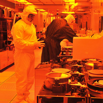
Sandia’s silicon fabrication facility in Albuquerque has been accredited by DoD to provide “trusted foundry” services for both unclassified and classified integrated circuits. The foundry accreditation increases the scope of Sandia’s existing accreditation for design services. (For that information, see the Sandia news release dated March 12, 2009, at www.sandia.gov/news/ resources/releases/2009/trusted_design.html).
Sandia’s Category1A status, which requires the most stringent protection measures, was awarded through the Trusted IC Supplier Accreditation Program of DoD’s Defense Microelectronics Activity.
The accreditation program is part of DoD’s strategy to ensure that electronic components used in US military and national security applications are trustworthy. Certification is necessary because the increasing offshore migration of all sectors of the microelectronics industry comes at a time of increasing demand for high-performance, application-specific integrated circuits (ASICs) from military and national security agencies.
The trusted foundry accreditation is for Sandia’s strategically radiation-hardened, 3.3-volt, 0.35-micrometer, silicon-on-insulator (SOI) CMOS process that produces custom low-volume, high reliability ASICs. Sandia’s silicon fab is optimized for radiation-hardened, analog and mixed-signal microelectronics, custom digital ASICs, and discrete devices.
Sandia uses 0.35-micrometer geometry to optimize performance for analog circuits resulting in better device matching, higher supply voltages, and broader signal dynamic range than smaller geometry devices. Properly designed and fabricated, larger devices are more likely to continue to perform in extended operating environments including temperature, shock, and radiation.
In support of its primary mission as steward of the US nuclear stockpile, Sandia has developed and delivered microelectronics products for nearly three decades. This expertise has also been applied to other national security needs. These include ensuring the nonproliferation of nuclear weapons and materials, reducing the threat from chemical and biological weapons, and providing advanced custom designs for other agencies like DoD. Sandia’s ASIC development team provides custom microelectronics products and engineering services that fulfill the needs of a diverse set of customers.
Sandia focuses on high-reliability custom solutions for high-consequence applications. An efficient ISO 9001-certified process is said to enhance chances for first-pass silicon solutions. “Sandia offers a total supply chain solution for radiation-hardened integrated circuits and microsystems by combining trusted ASIC design and fabrication with other in-house capabilities in packaging, test, failure analysis, and reliability,” says Gil Herrera, director of Microsystems Science Technology and Components Center 1700.
For more information or questions, visit www.sandia.gov/mstc or email Trusted_ASIC@sandia.gov.
