Once again defying a world rampant with cost overruns and unmet deadlines, Sandia’s massive MESA project will hold a building dedication at 10:30 a.m., Friday, April 21, to celebrate the formal opening — on-time and on-budget — of its Microfab and Microlab facilities.
Senators Pete Domenici and Jeff Bingaman, Rep. Heather Wilson, NNSA Defense Programs head Tom D’Agostino, and Sandia President Tom Hunter are among those slated to attend.
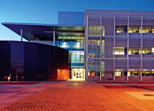
The Microlab building, attached by a second-floor skywalk to Sandia’s Microelectronics Development Laboratory at the southeastern end of Tech Area 1, is possibly the most architecturally scenic building Sandia has yet built, as well as the most secure.
Ringed by closely spaced boulders to protect against vehicular security incidents and using for the most part only basic materials like cement, steel, and glass, the imaginative, esuriently design — with light coming in from external walls of glass and large skylights three stories above the building’s central corridor — is expected to encourage interactions among groups formerly separate in the Sandia work force.
These include microelectronics workers in both silicon and compound semiconductors as well as computer visualization researchers. The intent is to combine the expertise of the three groups to more quickly imagine and design better microelectronic devices. These, produced in the MESA facility itself, would improve US security and also produce designs and methods that later might be found suitable for the consumer needs of US industry, which could use commercial manufacturing plants to produce products in the large numbers needed to satisfy a mass market.
The MicroFab replaces Sandia’s aging Compound Semiconductor Research Laboratory. The new three-story facility is one of the most modern and complex buildings at Sandia and was the first of three new facilities that make up the MESA complex. Its structure includes sophisticated safety systems and controls because of the hazardous materials used in the production of compound semiconductors.
Still to be completed for the MESA project is the Weapons Integration Facility, expected to be structurally finished later this year and operational in FY 2008.
The Microsystems and Engineering Sciences Applications (MESA) construction project supports the NNSA Defense Programs mission for research, development, and simulation. Upon completion, MESA is expected to provide the essential facilities and equipment to enable the design, integration, and qualification of microsystem technologies for the nuclear weapons complex of the future.
There have been no increases to the total project cost, project schedule, or original scope objectives since the project was originally baselined in October 2002.
Leading the way are Mike Cieslak, MESA Program Director, and Bill Jenkins, MESA construction project manager.