Sandia researchers create 3-D metasurfaces using III-V semiconductors
Last night I saw upon the stair/A little man who wasn’t there/He wasn’t there again today/Oh, how I wish he’d go away.
—From the poem Antigonish, by William Hughes Mearns (1899)
Like the little man upon the stair, metamaterials don’t exist in nature, but unlike him, no one wants them to go away. Formed by nanostructures that act as “atoms,” or unit cells, arranged on a substrate to alter light’s path in ways no ordinary material can achieve, these surrogate substances can manipulate an incoming light beam’s characteristics to enable more efficient versions of already known devices — optical filters, lasers, frequency converters, and beam steering devices, for example. They might create ultra-thin lenses and ultra-efficient cell phone antennas, bend light to keep satellites cooler, and make photovoltaics more efficient by enabling the absorption of more energy. They offer, in short, a world of possibilities.
One problem restraining extensive commercial use of this technology is limitations imposed by the materials composing them. Metal-based metamaterials are lossy at shorter wavelengths and can only operate effectively at low frequencies, such as the radio frequencies used by radar, before being overwhelmed by their own absorption. Silicon doesn’t emit light and can transmit it only in a limited wavelength range because of its narrow bandgap. Neither material can create a metamaterial that will operate in the infrared and optical ranges.
Optical metamaterials enter the arena
Now Sandia researchers have published technical papers — three in the past year — that are helping lead the way to the use of III-V semiconductors as the building blocks of metamaterials. More efficient than metals for optical metamaterial applications, with wider bandgaps than silicon, the III-V work featuring materials like gallium-arsenide and aluminum-arsenide is promising enough to have been featured by covers for two technical journals. (III-V refers to columns in the periodic table of elements.)
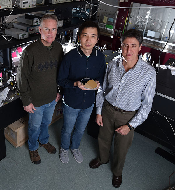
“There is very little work worldwide on all-dielectric metamaterials using III-V semiconductors,” says Igal Brener (1765), who has led the Sandia work with Mike Sinclair (1816) and Sheng Liu (1765). “Our advantage is Sandia’s vast access to III-V technology, be it growth or processing, so we can move pretty fast.”
Shinier than gold
The new Sandia dielectric materials not only lose little incoming energy but can even be fabricated in multiple 3-D layers to form complex meta-atoms that reflect more light than shiny gold surfaces, usually considered the ultimate in infrared reflectivity. The III-V materials also can emit photons when excited — something that silicon, which can reflect, transmit, and absorb — can’t do. Another advantage of these dielectric materials is their highly nonlinear responses, enabling the generation of light at different colors that could be used for extending the wavelength range of lasers or for generating “entangled photons” for quantum computing.
Another attractive aspect of the Sandia approach is the relatively simple method of forming the artificial atoms, known as resonators, that are the guts of the metamaterial.
To confine light, you need a high refractive-index contrast.
Created under the supervision of Sheng Liu, hired as a post-doc five years ago and converted to staff a year ago, the meta-atoms are a few hundred nanometers in diameter and composed of many actual atoms. One of Sheng’s insights was to oxidize these tiny groupings around their perimeters to create layered coatings with a low index of refraction, rather than use a more expensive, time-consuming “flip-chip” bonding process. The complexity of previous methods was an obstacle to cost- and time-efficiency in achieving the same result. His simplification, he says, previously had been used by other researchers in 1700 to make lasers, but not metamaterials.

The oxidized, low-index surface surrounds the high-index core “like in winter time, you have a coat surrounding you,” Sheng says. “To confine light, you need a high refractive-index contrast.” Put colloquially, interior light bumping into the low-indexed oxide surface is herded back by the refractive difference into travelling along the high-index core.
Gordon Keeler (1764) achieved controlled oxidation simply by putting III-V materials in a hot oven and flowing water vapor over the sample. “It will oxidize at a certain rate,” Sheng says. “The more material, the longer it takes.”
The manmade meta-atoms are sculpted in place during a lithographic process that permits researchers to make whatever pattern they chose for the placement of the metamaterial components. “We use simulations to direct us,” Sheng says. Spacing to some extent is determined by the size of the manmade atoms.
Fractured cubic nanostructures store unusually large amounts of energy
The researchers experimented with cylindrical and cubic nanostructures, reducing the symmetry of the latter to achieve even better properties.
“Cylinders are much easier to fabricate and typically can be used for conventional metasurfaces,” says Igal. “But in the ACS Photonics paper [that concerned cubic shapes], broken symmetry cubes are crucial to obtain very sharp resonances. That’s the key issue of the paper.”
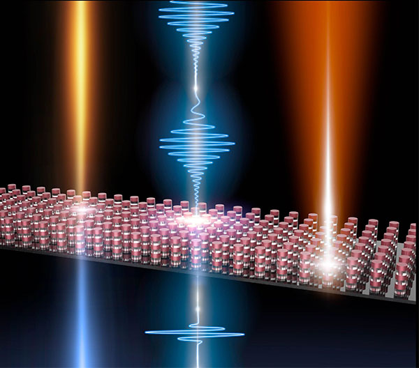
The idea of intentionally reducing the symmetry of a cubic resonator nanostructure originated five or six years ago, says Mike, with a serendipitous design that happened to break the intentionally symmetrical shape of the meta-atoms in an attempt to mimic a possible manufacturing flaw. “During a Grand Challenge Laboratory Directed Research &?Development (LDRD) project on metamaterials, when we were first fabricating cubic resonators in our effort to see if we could get beyond microwaves into infrared and optical metamaterials,” says Mike, “we were playing with the shape of resonators to try to simulate the effect of lithography errors. In one simulation, we happened to cut a corner of the cube and all of a sudden very sharp reflection bands appeared.” Prior to that discovery, dielectric resonator metamaterials only showed broad bands that didn’t trap much energy. The researchers found that the new sharp resonances allowed larger amounts of energy to be stored in the design — beneficial for efficient frequency conversion, and perhaps even for light emission and lasing.
The exploration of the crimped resonator didn’t fit under the Grand Challenge, and was explored later under the auspices of DOE’s Basic Energy Science office. Salvatore Campione, building on previous work by Lorena Basilio, Larry Warne, and William Langston (all 1352) used electromagnetic simulations to unravel precisely how the cubes trap light. Willie Luk (1131) measured the cubes’ reflective properties. Another LDRD project currently supports research into metamaterial lasing.
“We feel we’ve created a pretty flexible platform for a lot of different kinds of devices,” says Mike.
The ongoing work is aided by John Reno (1131), nationally known for growing extremely precise crystalline structures, who contributed the III-V wafers.
?Three patents on aspects of the work have been submitted to the US Patent Office.
A large part of the work took place at the Sandia/Los Alamos Center for Integrated Nanotechnologies, a DOE Office of Science user facility.
Three papers of interest led by Sandia researchers
- Nanoletters, Resonantly Enhanced Second-Harmonic Generation Using III?V Semiconductor All-Dielectric Metasurfaces
- Advanced Optical Materials, Dielectric Resonators: III–V Semiconductor Nanoresonators—A New Strategy for Passive, Active, and Nonlinear All-Dielectric Metamaterials“.
- ACS Photonics, Broken Symmetry Dielectric Resonators for High Quality Factor Fano Metasurfaces“