
On a beautiful summer morning, under a tent with rolled-up sides to allow air flow, approximately 100 attendees celebrated the completion of the $518 million Microsystems and Engineering Sciences Applications (MESA) project in a formal dedication on Aug. 23 at Sandia.
Among those speaking were Sen. Pete Domenici, R-N.M., DOE Deputy Secretary Clay Sell, NNSA Administrator Thomas D’Agostino, Sandia President and Labs Director Tom Hunter, and Sandia Deputy Director for Nuclear Weapons Joan Woodard.
The 400,000-square-foot complex was completed in eight years — three years ahead of schedule — and $40 million under budget.
It consists of three discrete buildings: the Microelectronics Development Laboratory and MicroFab, the Microsystems Laboratory, and the Weapons Integration Facility.
It will combine the most advanced design and simulation tools and the most advanced microsystems and nanotechnologies to meet NNSA mission requirements.
Said Labs Director Tom Hunter, “This is an event that truly defines this institution. [It will mean] unquestioned technological leadership in the synthesis of the almost unlimited potential of integrated microsystems and the awesome power of the world’s fastest computers.
“We could have conceded to the easy, taken the road more traveled, [joined with those who are cutting back on their expectations] but not doing so has made all the difference. We join with the yea-sayers — those who had the commitment and conviction to see [this project] done.”
Every speaker praised the team that had completed the complex under budget and ahead of time.
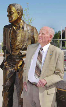
Also unveiled was a seven-foot-tall bronze statue of retired Sandia engineer Willis Whitfield, inventor of the “clean room” technology that made modern microelectronics production — and therefore MESA itself — possible, as well as hospital surgery rooms safer (see “Statue of clean room inventor Willis Whitfield unveiled at MESA opening,” page 6).
The MESA ceremony, which involved both a ribbon-cutting for the buildings and unveiling of the statue, took place at the heart of the space in which the three physically beautiful buildings are housed.
In addition to fabricating electronic circuits, the MESA facility also makes microelectromechanical systems (MEMS) for advanced security systems, sensors, guidance systems, and other applications.
The complex also includes the world’s most complete compound semiconductor fabrication facility. This will produce advanced optoelectronic and custom electronic components for sensors, communications, quantum computing, and other emerging technologies.
While the facility is designed to support NNSA missions, it is expected to have a broad impact on national security technologies beyond nuclear weapons and meet the technical challenges faced by several government agencies. MESA is also expected to be a major scientific research center for micro- and nanotechnologies, and contribute to international competitiveness through partnerships with US companies.
MESA: In simple terms, what it is
Because abstract terminology sometimes conspires with nonreleasable information to make basic Sandia work not as readily understandable as it could be, here is a summary in down-to-earth terms of the importance — current and expected — of MESA.
The MESA project has nuclear origins and financing but projected larger ends.
Nuclear weapons
A major concern of nuclear weapons as a deterrent to enemy attacks is that these potent weapons be protected against circuit failure caused by radiation.
Sandia’s job is to analyze where that radiation might cause failure and protect against it.
The circuitry of a weapon sits within the weapon warhead, itself a radioactive source, for decades.
A launched missile passing beyond Earth’s protective atmosphere exposes circuitry to the harsh radiation of outer space.
Reentering Earth’s atmosphere near a potential target, an adversary with even a tiny nuclear arsenal might feel he has nothing to fear from these weapons because he could explode a nuclear weapon of his own in Earth’s atmosphere. This would emit various forms of radiation, electromagnetic pulses, and pressure bursts from shock waves that would decommission the circuitry of any incoming nuclear weapon, essentially turning it into a dud.
The blast could also disable communications satellites, leaving US military planners blind.
A blast over the continental US could achieve the same ends.
To remove any doubt of the effectiveness of US retaliatory nuclear weapons or its satellite information system, MESA’s upgraded silicon fabrication facility makes chips that retain function in extreme radiation environments.
The number of these ‘hardened’ circuits needed in weapons and communication satellites is too small and has too stringent a set of requirements to interest an industrial chip manufacturer. So Sandia is the supplier of these circuits, built at MESA, for defense needs.
“We physically made the chips here that will go into the W76-1,” says MESA director Mike Cieslak.
Why redo them? “The physics package is fine,” says Mike. “But our electronic systems are getting older than my kids. Who has the same cell phone or computer, the same oil in their car, as they did five years ago?”
And time has brought social changes as well.
“Since 9/11,” says Mike, “there’s been a reassessment of security threats against many things — metros, power plants, and so on, as well as nuclear weapons. We want our weapons and facilities secure against threats we haven’t even imagined till now.”
All of MESA, he says, will be available to that purpose.
“We’re developing technology options applicable either to RRW or any lifetime extension (the refurbishment of old weapons) deemed by Congress to be appropriate.”
The point to deterrence, he says, is that foes know the weapons would work as designed if used.
“The mission,” he says, “is deterrence.”
Only system studies, not system designs, will be made for the more advanced weapons systems at this time.
Further defense factors
But while weapon survivability is important, so are other factors.
Surveillance devices that can help assess the reliability of these weapons can be built in MESA’s facilities, which include silicon and compound semiconductor materials fabrication. Devices manufactured in these fabs also help monitor subways and ports for dangerous chemical, biological, and radiological devices. A small area permits joint fabrication between the different classes of materials — the only such facility known in the world.
MESA is also available to be a trusted foundry for national security products required by other government agencies such as DoD and others.
“We’re defending against people very different from ourselves,” says Mike. “Our job at Sandia is to imagine every way someone like that could attack us, and create ways to address that possibility.”
Innovative collaboration
Finally, the buildings and their researchers in MESA’s unclassified areas will design innovative products in collaboration with industry and academia. The collaboration helps American companies, as in the much praised collaboration with Goodyear Tire, and also helps national defense.
“Rubber parts aren’t only on tires,” says Mike. “They’re the O-rings and gaskets of our weapon systems. And we use polymeric foams and encapsulants in all of our weapon systems.”
To accomplish this end, MESA has continued its innovative approach of placing researchers from various Sandia line organizations next to each other — if not cheek by jowl, at least in the same common area — instead of maintaining the traditional Sandia approach of pairing like with like from the same organization.
“We did this in our prototype MESA facility (MESA-TOP),” says Mike, “and it worked very well at accelerating the pace of development.” Researchers maintain membership in their line orgs, where their work is still judged.
Research areas in which MESA participates include fluidics, thermal, mechanical, structural, and electrical. The work will involve computational simulations, engineering design, and actual production of parts. Microsystems involving microdevices (such as the gold louvers providing shade for NASA satellite components) as well as microcircuits are included under the MESA umbrella.
“We want to assure the safety, security, reliability, and survivability of our components and weapon systems,” says Mike. “We’d like to be able to have a ‘check weapons’ display like we currently see ‘check oil’ on our dashboards.”
He’s looking for MESA to provide this.
Statue of clean room inventor unveiled
Textbooks usually don’t mention the origin of the clean room technology that makes the modern microelectronics age — let alone nanotechnology — possible. Or they give passing credit to NASA or Bell Labs.
But patents for the clean room were issued in 1962 to Sandia’s Willis Whitfield, who enjoyed some celebrity throughout the 1960s for the achievement. He hobnobbed with astronauts. He was sought after by industrialists wanting to lessen production failure rates as high as 50 percent in the increasing number of enterprises requiring electronics. His work was a factor in significantly lowering infection rates in hospitals because the invention improved the cleanliness of surgery rooms.
It was a small thing to Willis. In his own mind, it was not one of his greater achievements. He simply examined the systems available at the time that were used to keep rooms clean. These included ideas that seem bizarre today: walls sloped to hinder dust from settling on them; perpetual, minute-by-minute maintenance by janitors wielding cleaning cloths. The problem, of course, was that the dust — small by ordinary human standards — loomed big as boulders in etching processes as circuits grew smaller, increasing industrial component failure rates. Many solutions were proposed but nothing sufficed.
Then Willis devised the system still in use today. Like many noteworthy ideas, it was simple. Among the increasingly convoluted efforts of the time, the idea was, you might say, a breath of fresh air. Air, in fact, would be his janitor. By blowing cleansed, monotemperature, unidirectional air not only into the room but through louvers leading from it, he was able to clean rooms yet avoid whorls that would send dust spiraling and depositing. The method, on its initial tests, left rooms a thousand times cleaner than ever before, and that was just the start.
Today the patent — let for free by the Atomic Energy Commission, which oversaw Sandia at the time — is used around the world so casually that few remember the technique had an inventor.
And Willis, who lives quietly with his wife in Albuquerque’s Northeast Heights on a Sandia pension, is more or less anonymous in the world and happy with that status.
But without Willis, there might not have been a MESA. So Sandia decided to honor the quiet inventor, and through him, all engineers, with a unique response: a seven-foot-tall representation of him at the heart of Sandia’s largest project. He is the only Sandian — and one of very few engineers worldwide — ever so honored with a statue.
The statue was unveiled at the MESA ceremonial opening.
Funded by Lockheed Martin and sculpted out of bronze by former Sandian Neal McEwen, it sits outside, near the ceremonial fountain of the MESA center, a testimony to the effect of engineering on the future of humanity.
“I made him bigger than life, in a somewhat casual pose, like a college professor sitting on one edge of a desk lecturing a class, to convey someone with authority but approachable,” says Neal. “We wanted to honor engineers in general through a representation of Willis.”
The document near Willis’ hand is a copy of his initial drawing of a clean room.
Says Sandia Executive VP John Stichman, “We’re fortunate that one of our own invented the absolutely key enabling technology known as the clean room. As a laboratory known for solving important, complex problems through engineering excellence, it is fitting that we honor engineers and this special person on this site. We are especially grateful that Lockheed Martin is sponsoring this tribute.”
At the statue’s base is a brief summary of Willis’ work, and a quote from President Dwight Eisenhower: “Engineers build for the future, not only for the needs of men, but for their dreams as well. Thus, inherently, the engineer’s work is a fearless optimism that life will go forward, and that the future is worth working for.”
MESA fact sheet
- MESA is the largest federal investment in computationally enabled microtechnologies worldwide, with an original budget of $518 million.
- The 400,000-square-foot complex was completed in eight years, three years ahead of schedule and $40 million under budget.
- More than 600 people will work at the MESA fabrication facilities continuing Sandia’s long history of miniaturizing and integrating emerging technologies to build useful and sometimes novel hardware.
- MESA is the first fabrication facility in the world to integrate silicon and compound semiconductor materials. Silicon is used in computer chips for its electrical transmission and insulation properties. Compound semiconductors like gallium arsenide and its sister materials are used for radio frequency and optoelectronics — the more exotic, complex material of choice for devices that use light rather than electrons.
- MESAs fabrication facility makes electronic circuits and computer chips that can survive assault by radiation. These so-called hardened electronics are not obtainable elsewhere. They offer security that an adversary will not explode a nuclear weapon in the atmosphere to wipe out US satellite communications or render US retaliatory weapons into duds by frying their electronics.
- The center can also provide a secure foundry for electronics and optics required for sensors designed by other US agencies.
- Access to high-performance computing simulations should make MESA a world leader in a new type of simulation-led engineering that will ultimately improve the quality of consumer goods.
- Discussion of the project began in July 1999. The design package was submitted to DOE the day before Sept. 11, 2001. Final DOE signoff was achieved in June 2007.
- For the technically inclined: MESA interests will include strained-layer superlattices, multilevel silicon sacrificial surface micromachining, photonic lattices, microfluidics, and nanotechnology discovery platforms.