The Nanoelectronics and Nanophotonics group uses a combination of experiment, theory, and modeling to discover and exploit the unique properties of nanomaterials for electronics, photonics, and optoelectronics.
In addition to addressing scientific and technical challenges from nanoscience to nanotechnology, our team of materials scientists, physicists, and chemists enjoys pondering the quirkier side of science, as can be seen in the Entropyman website created by postdoctoral researcher Edward Feng.
Our group also likes to spend time together outside of the research environment.
Announcements
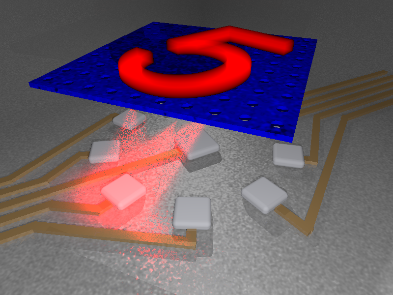
Optical Neuromorphic Computing
Classification of features in scenes is important for many applications. Typically this is done by capturing images with cameras and analyzing the content with computer algorithms. Here we study a different approach where a passive material directly performs a neuromorphic task, with significant potential reduction in energy and time.
Origami Terahertz Detector
We present a new approach for fabricate terahertz detectors by inkjet printing of carbon nanotubes on ultrathin substrates. These detectors can be folded to create 3D structures that improve performance and can be used for imaging. This opens up a path for future detectors that are foldable, insertable, and deployable.
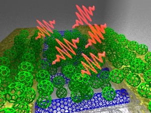
Ultrahigh gain phototransistor
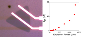
Detection of low light intensity down to the few photon level requires photodetectors with high gain. We introduce a new type of photototransistor based on aligned carbon nanotube arrays functionalized with C60. We achieve a gain greater than 108 at room temperature, and demonstrate the detection of as few as 50 photons per carbon nanotube.
High efficiency thin film thermoelectric cooler
Thin film thermoelectric coolers are promising for localized cooling in electronics. However, the contact resistance becomes a limiting factor when the films are only a few tens of microns thick. In collaboration with RTI, we developed a new modeling-predicted approach to making contacts to thin film superlattices, leading to a 100-fold reduction in the contact resistance, and significantly improved cooling.
Alec Talin elected APS Fellow
The American Physical Society announced its 2017 Fellows and Alec was recognized “For the discovery of new electronic transport phenomena, materials, and devices.”
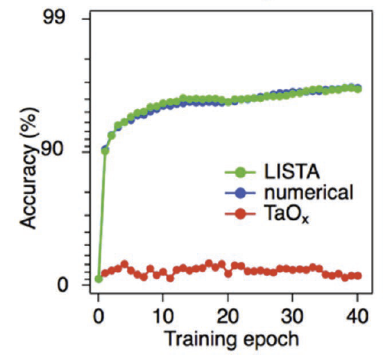
Neuromorphic computing: harnessing battery materials
Our research group has developed a new device concept for neuromorphic computing based on materials utilized in solid-state batteries. The new concept uses the insertion of Li in LCO to dynamically control the LCO conductivity, leading to an analog device where hundreds of stable states can be written. Simulations based on the experimental data show record learning capability. The paper, published in Advanced Materials.
François Léonard elected APS Fellow
The American Physical Society announced its 2016 Fellows and François was recognized for “Fundamental studies of the physics of nanoscale electronic devices”.
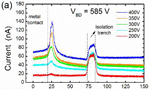
In-Operando imaging of edge termination electric fields in GaN power devices
High-power devices based on GaN show promise for a number of potential applications. To realize this promise, it is essential to manage the electric fields to prevent early breakdown, which is accomplished using edge terminations. Unfortunately, the effectiveness of edge termination designs is usually only inferred through indirect means, such as the impact on the breakdown voltage. In a paper in IEEE Electron Device Letters, we show how scanning photocurrent microscopy can be used to characterize the inner workings of the edge termination while large voltages relevant to high-power electronics are applied. The measurements reveal a rich dynamic behavior.
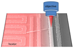
Simultaneous thermoelectric and optoelectronic characterization of individual nanowires
We present a measurement platform to simultaneously perform thermoelectric and optoelectronic measurements on the same individual nanowire. An example application to GaN/AlGaN core-shell nanowires reveals the spatial and temporal coexistence of photothermoelectric and photogating mechanisms. See the paper in ACS Publications – Nano Letters.
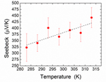
Thermoelectric metal-organic framework
We present the first demonstration of thermoelectricity in a metal-organic framework (MOF) material. We find a large Seebeck coefficient at room temperature and low thermal conductivity, two important properties for making efficient thermoelectric devices. This work opens a path towards new types of thermoelectric materials based on molecular, long-range ordered, nanoporous materials. See the paper in Advanced Materials.
Superlinear photocurrent in 2D materials
In most materials, the photocurrent usually depend linearly or sub-linearly on light intensity due to conventional recombination processes. Several decades ago, a few exotic materials displayed an unusual superlinear increase of the photocurrent with increasing light intensity, which stumped theorists for a long time. We report the experimental observation of this intriguing regime in novel two-dimensional transition-metal dichalcogenides. This behavior is observed in monolayer alloys spanning the compositional range from MoS2 to MoSe2, and is suggested to arise from the non-equilibrium photophysics of multiple recombination centers. See the paper in ACS Publications – Nano Letters.
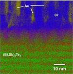
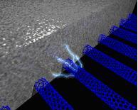
Electrical contacts to topological insulators
Topological insulators possess unique electronic and optical properties of interest for novel devices. To realize this promise, it is important to achieve high-performance electrical contacts. In a recent paper, we employ large-scale ab initio calculations to demonstrate the many features of such contacts. In particular, we find that strong interaction between the metal and the TI destroys spin-momentum locking, in contrast to the commonly accepted view that TI states are robust.
Carbon nanotube terahertz detector
In a collaboration with Rice University and Tokyo Tech, we demonstrated a macroscopic, antenna-free, terahertz detector based on thin films of carbon nanotubes. The detector is broadband, does not require power to operate, and shows performance approaching that of established uncooled technologies. Additional details can be found in the journal Nano Letters and in this video.
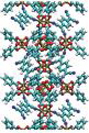
Electrically conducting metal-organic frameworks
In a new paper in Science, our group demonstrates for the first time electrical conductivity in a metal-organic framework (MOF). By infiltrating the HKUST MOF with guest molecules, we tuned the electrical conductivity over six orders of magnitude in thin film MOF devices. In addition to creating a new class of conducting nanoporous materials, this work opens up new avenues for applications in sensors, electronics, and optoelectronics.
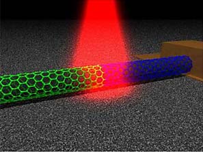
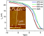
Carbon nanotube p-n junction photodetector with intrinsic polarimetry
We developed a novel approach to create macroscopic carbon nanotube p-n junction photodetectors based on the photothermoelectric effect which shows polarization sensitivity up to the mid-infrared. The experimental work in conjunction with theory establishes the working principles and performance attributes of this class of devices. The paper was recently published in ACS Nano DOI: 10.1021/nn402679u.
Broadband carbon nanotube photodetector
In a recent paper in Nature’s Scientific Reports, we present a broadband photodetector based on thin films of aligned carbon nanotubes. The detector shows good linearity from the visible to the mid-infrared, and because of the unique aligned-nanotube material, opens a new path for polarimetry.
Physical removal of metallic nanotubes from nanotube network devices
Electronic and optoelectronic devices based on carbon nanotubes are limited by the presence of metallic nanotubes in addition to the desirable semiconducting nanotubes. Our group, in collaboration with Rice University, devised an approach to physically remove the metallic nanotubes from devices post-fabrication using functionalization combined with a thermal and fluidic process. Details can be found in the journal Nanotechnology.
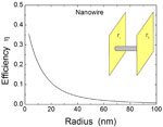
Themoelectric efficiency in the space-charge-limited transport regime in semiconductors
The thermoelectric efficiency of materials is usually considered at high doping where the electronic transport is ohmic, leading to the conventional ZT factor. In a new theoretical paper published in Physical Review B Journal, we derive the equivalent thermoelectric efficiency for low doping where the electronic transport is dominated by space-charge-limited effects. Application to specific systems shows that nanowires are the most promising to harness this regime.
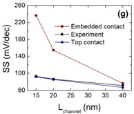
Gate modulation of contacts improves performance of carbon nanotube transistors
The performance of field-effect transistors degrades as the channel length is reduced unless the gate oxide thickness is aggressively scaled. In a recent paper in ACS Nano we demonstrate that these scaling issues can be overcome in short channel carbon nanotube transistors by allowing the gate to modulate the contacts. Enhanced Performance of Short-Channel Carbon Nanotube Field-Effect Transistors Due to Gate-Modulated Electrical Contacts.

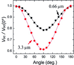
Anisotropic intrinsic spin Hall effect in quantum wires
A recent paper in J. Phys.: Condens. Matter 23, 465301 (2011), discussed the impact that crystallographic orientation has on the strength of the intrinsic spin Hall effect in GaAs quantum wires. An image from this paper was featured on the cover of the journal’s November 23 issue.
Electrical contacts to one- and two-dimensional nanomaterials
Electrical contacts play a critical role in many technology areas, and understanding contacts to nanomaterials is essential to fully harness their technology potential. A review article from our group details the unique issues associated with such nanocontacts. Nature Nanotechnology 6, 773 (2011).
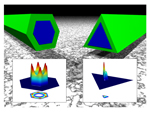
Nanoscale Effects on Heterojunction Electron Gases in GaN/AlGaN Core/Shell Nanowires
As detailed in a recent paper in Nano Letters 11, 3074 (2011), the electronic properties of heterojunctions are significantly different in core/shell nanowires as compared to their bulk form, leading to the formation of quasi-one-dimensional electron gases.
Congratulations! Aaron Katzenmeyer has received his Ph.D. in Electrical and Computer Engineering from the University of California, Davis. Read Novel Electrical and Optoelectronic Characterization Methods for Semiconducting Nanowires and Nanotubes PDF if you would like to read his dissertation.
Nanoelectronics and Nanophotonics group receives LDRD Award of Excellence.
A project from our group titled “Energy Conversion Using Chromophore-Functionalized Carbon Nanotubes” was recently awarded a 2010 LDRD Award for Excellence for its embodiment of “National Laboratory Challenge, Risk and Creativity,” and “National Laboratory Relevance and Impact.”
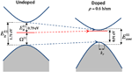
Tunable Band Gaps and Excitons in Doped Semiconducting Carbon Nanotubes Made Possible by Acoustic Plasmons
We studied the impact of doping on the electronic and optical properties of semiconducting carbon nanotubes, as discussed in Phys. Rev. Lett. 104, 177402 (2010).
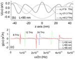
Terahertz response of carbon nanotube transistors
We developed a new approach to calculate the high frequency properties of nanoelectronic devices, as described in Phys. Rev. Lett. 103, 026601 (2009).
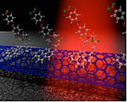
Our group recently demonstrated that chromophores/nanotube hybrid devices can detect different colors of light. See this featured in Nature Photonics.
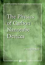
François’s book, The Physics of Carbon Nanotube Devices, has been released!
“…the definitive text on the topic”
—ScienceDaily, May 29, 2008
This book explains the basic physics of carbon nanotube devices for multiple applications including electronics, nano-electro-mechanical systems (NEMS), and optoelectronics.
For more information about The Physics of Carbon Nanotube Devices.