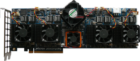
On July 17, 2014 representatives from Sandia, LBNL, PNNL, and DoD’s LPS/ACS organizations met with Micron to discuss the Multi-FPGA application development environment, and the status of memory controller updates for the Micron hybrid memory cube (HMC) test and evaluation (T&E) boards. Initial Micron testing demonstrated approximately an order of magnitude improvement in performance on the giga updates per second (GUPS) benchmark using the HMC memory versus third generation, conventional dual data rate (DDR3) memory. After initial testing of these prototypes by Micron, eight test and evaluation boards were produced under a Sandia contract for DOE—for both the ASC and ASCR program offices. A DS&A WFO program subsequently order two additional T&E boards. Micron presented NDA information for integration of HMC technology into compute node designs. Sandia, LBNL, PNNL and LPS/ ACS agreed to share lessons learned and documents to help each other develop application tests and benchmarks among our group.
On July 18, 2014 Sandia held a kickoff meeting at Micron for new DOE ASC and ASCR R&D project. This project is focused on three design studies based on HMC technology. The first two design studies are focused on system R&D for functions in memory cubes, and for integration of cubes into resilient memory modules. The third design study is focused on an analysis of search operations in a HMC or HMC module. To support this R&D, Micron is also designing and producing two additional T&E boards, a small board with a single FPGA and a single HMC for application development, and a board with two HMCs and two FPGAs that is designed for analysis of chaining and module integration protocols. Sandia provided advice to Micron on the specific R&D topics that would have the greatest potential impact for HMC in DOE systems.