As supercomputing systems evolve toward ever higher levels of performance density, their continued advance is threatened by looming fundamental thermal limitations. Historical performance improvements were largely enabled by increases in energy efficiency, which will soon slow down as the low-hanging fruit will have been plucked. Continued progress beyond this point would require the use of an unconventional approach called reversible computing, to conserve energy in digital systems by conserving information. Research at Sandia is investigating the viability of this approach.
Over the last several decades the overall performance rating of leading HPC systems in floating-point operations per second (FLOPS) has increased steadily, from teraflops in the 90s to over an exaflop today. This increase would not have been feasible if not for significant improvements in the energy efficiency of digital technologies. The astounding millionfold performance increase from the ASCI Red supercomputer in 1997 to Frontier today was achieved while only increasing power consumption by 25×; this corresponds to about a 40,000× improvement in performance per watt over the last quarter-century. About 200× of this relates to a reduction in the scale of digital signal energies, with minimum transistor gate energies having gone from about a femtojoule in the 1997 250 nanometer (nm) technology to around five attojoules in today’s leading-edge “three nm” fin field-effect transistors, or FinFETs, while the other 200× came from optimizations at higher levels in system design (architecture, packaging, memory, interconnects and software).
But now, further improvements across all these levels threaten to soon enter an era of diminishing returns. In particular, at the device level, transistor gate energies are only projected to decrease by around another 2× through further process improvements. These energies are limited by fundamental thermal noise considerations to no more than about a 50× reduction from today’s level, even if aggressive subthreshold voltage scaling techniques can be applied. The room left for optimization at higher levels in the technology stack is similarly limited. Hence, it seems unlikely that the rates of performance improvement that we have been accustomed to in digital computing can be sustained much longer if we persist in using conventional methods.
Among unconventional approaches to computing, only one offers the potential to increase the efficiency of low-level digital compute far beyond the fundamental thermal limits of conventional technology mentioned above: Namely, reversible computing. This approach, first conceived in the 1960s and ‘70s by pioneering researchers Rolf Landauer and Charles Bennett of IBM Research, stems from the observation that there is only a fundamental thermodynamic minimum on the energy that must be consumed to perform a digital operation if logical information is lost in the course of carrying out that operation. When logical information is conserved, the digital signal energies used to represent that information can, in principle, be recovered and reused as well; that is, we can theoretically approach the ideal of computing in a manner that is both logically and thermodynamically reversible.
The engineering challenges that would need to be addressed to approach this ideal in practice are formidable. Given the National Strategic Computing Initiative’s mandate to find a path forward beyond the limits of current technology, NNSA’s Advanced Simulation and Computing, or ASC, program has supported an effort at Sandia since 2017 to carefully assess the potential for further development of the reversible approach to feasibly carry digital computing efficiency beyond the end of the semiconductor roadmap. In parallel, a Laboratory Directed Research and Development, or LDRD, project started that year led to subsequent Strategic Intelligence Partnership Program, or SIPP, sponsorship of a complementary line of work to expand the scope of the team’s effort to include early-stage research into novel reversible superconducting technologies for digital compute.
A foundational aspect of this work has been to solidify the theoretical basis for reversible computing. In a series of papers, Sandia showed how the concepts of reversible computing can be generalized from traditional models to a more adaptable form suitable for practical computing hardware. Sandia clarified why the physical motivation for reversible computing follows rigorously from fundamental concepts of statistical mechanics and information theory. Briefly, because fundamental physics is reversible, discarded information cannot be destroyed, and instead it inevitably manifests as new physical entropy. Currently, in collaboration with university partners, the team is investigating the ultimate physical limits of reversible computing efficiency using theoretical tools from non-equilibrium quantum thermodynamics.
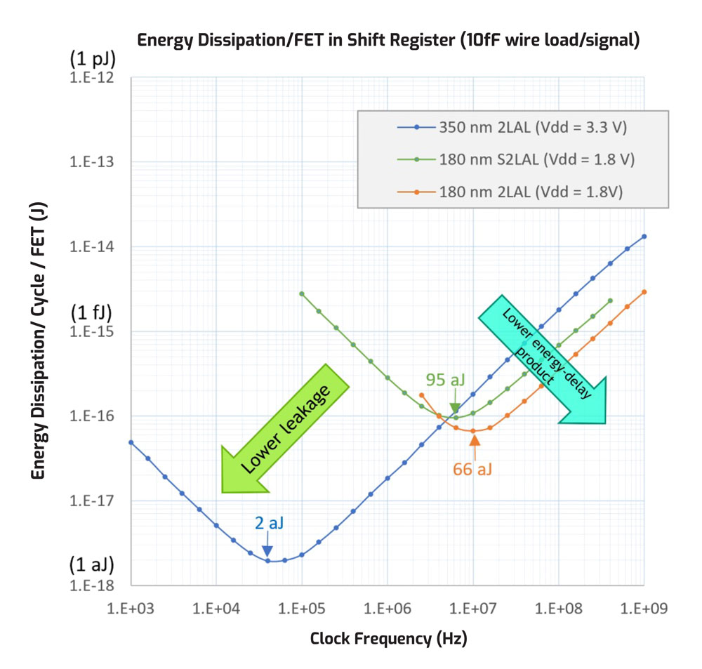
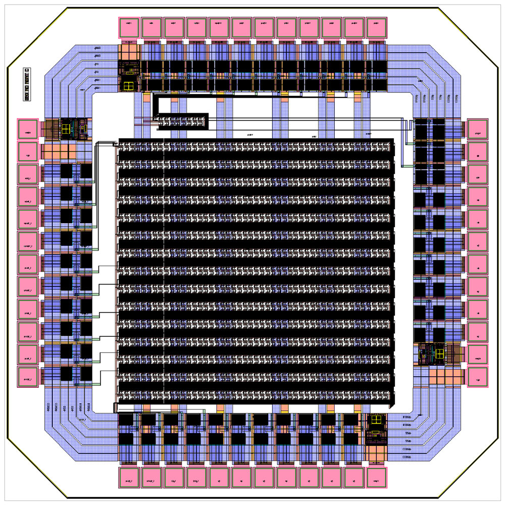
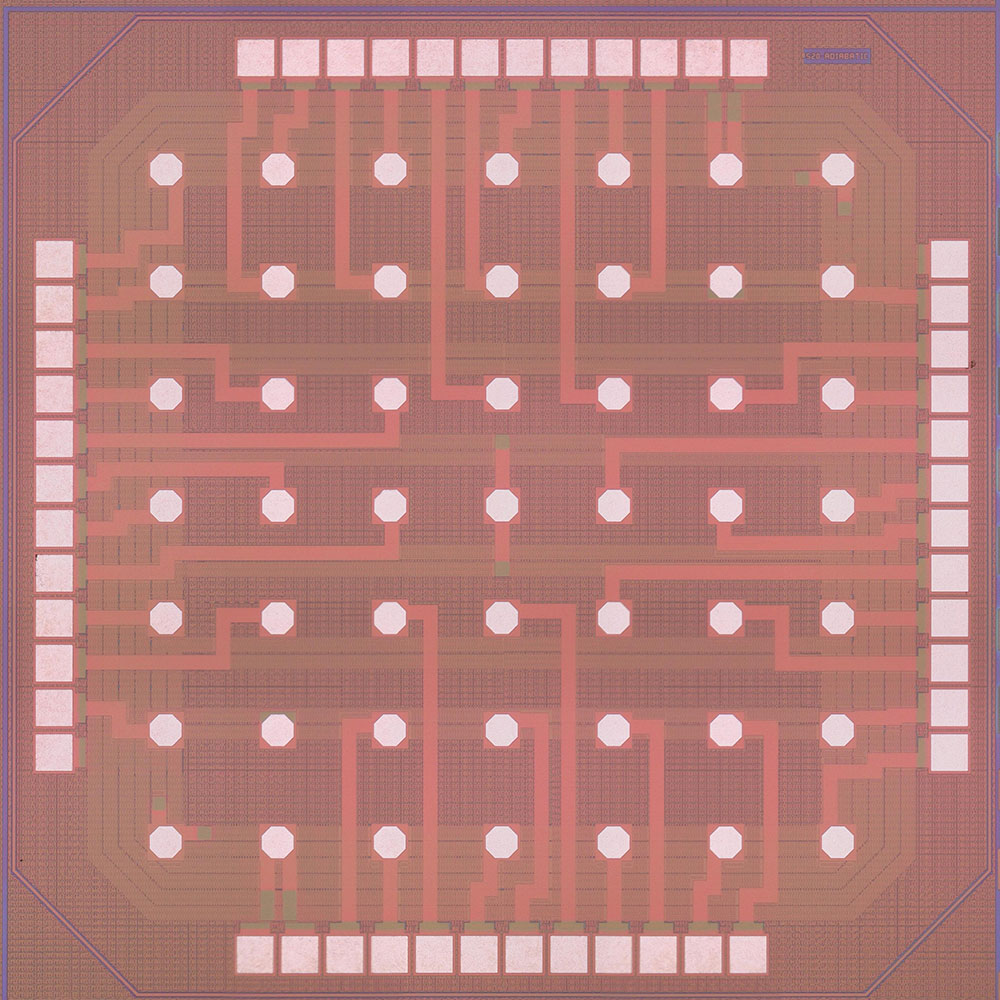
Building on the theoretical foundations, the central thrust of this work is to develop and analyze engineering implementations of these concepts. Sandia can implement reversible computing in existing CMOS technology via adiabatic switching based on alternative logic gate designs and clocking disciplines. While the basic principles behind this approach have long been recognized, past implementations were far from perfect. However, the team’s focus is to truly push the limits of this approach. Sandia’s major contributions in this area to date include: (1) the invention of a new complementary metal-oxide semiconductor, or CMOS, logic family that is perfectly adiabatic; (2) the design and fabrication of a test chip using Microsystems Engineering, Science and Applications, or MESA, 180nm process; (3) circuit simulations showing that raw efficiency gains of up to three orders of magnitude are achievable in MESA’s processes (beating even end-of-roadmap CMOS!); (4) the invention of a novel resonant oscillator circuit designed to recover >99.9% of the signal energy from an adiabatic CMOS chip; (5) a detailed analysis of the theoretical gains in raw efficiency and throughput density that could be achieved across future CMOS technology nodes, showing that >100× boosts in raw throughput density versus conventional CMOS should be attainable. Sandia’s work in this area continues, with results to date suggesting that, with further development, reversible computing technology could significantly benefit future HPC systems.
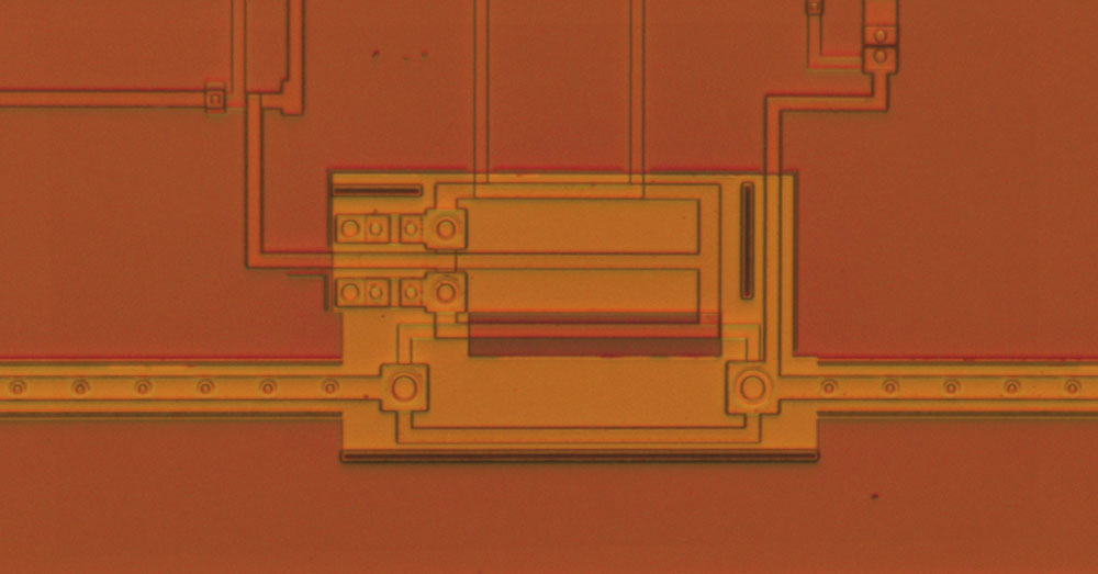
In a complementary line of work funded by external agencies, Sandia is looking farther ahead to investigate a novel approach to reversible computing. This approach is based on the ballistic transport and asynchronous elastic interaction of flux solitons, or fluxons, conveying single magnetic flux quanta in superconducting circuits based on Josephson junctions, or JJs. Superconducting approaches are interesting for their potential utility in applications at cryogenic temperatures, such as for the control and readout of superconducting qubits in quantum computing. This line of work is still at a very early stage of development, but important advances to date include a patented design concept for a single-JJ reversible memory, or RM, cell, a fabricated niobium test chip for this circuit, and an enumeration of possible primitive operations in our new Ballistic Asynchronous Reversible Computing in Superconductors, or BARCS, computing paradigm. The team’s future plans involve utilizing Sandia HPC resources for AI-enhanced automated discovery of additional BARCS circuits suitable for general-purpose computation.
In closing, the team’s work exemplifies Sandia’s dedication to innovation and addresses the national strategic need for groundbreaking efficiency in digital computation. This research, while challenging, helps to bolster the long-term contribution of Sandia National Laboratories to the national interest, and has enjoyed support from NNSA’s ASC program, Sandia’s LDRD program, and SIPP partners. Looking forward, the team anticipates continued progress and new discoveries in the quest to push the limits of energy efficiency in digital computation. The team will continue to leverage Sandia’s HPC resources to flesh out this novel approach to reversible computing, aiming to contribute not only to the field of HPC, but also to advanced applications and a more sustainable future. Consistent results and ongoing advancements in this field serve to reinforce confidence in this research and to affirm Sandia’s role in leading technological innovation.