Low-power sensors could last 10 years, providing surveillance, security
Imagine a smoke detector that instead of warning residents of smoke before a fire engulfs their home, is placed in mass-transit locations to alert travelers and first responders to hazardous chemicals in the air.
Researchers at Sandia have spent the last three years developing an ultra-low-power chemical sensor to detect sarin and other chemical warfare agents or gaseous industrial toxins, aiming to protect the public and warfighters.
Sarin is an extremely toxic nerve agent that can cause death within minutes. The production and stockpiling of sarin, along with other nerve agents and mustard gas, are outlawed. However, sarin has been used in terrorist attacks.
“When we’re thinking about ultra-low-power electronics, we want to install a sensor and leave it in the field for a long time,” said Mieko Hirabayashi, a Sandia microelectronics engineer and project lead. “We don’t want to worry about replacing the batteries often.”
Anyone who has changed a smoke detector battery in the middle of the night can appreciate the value of sensors that can operate for a decade without battery replacement.
Spongey sensor for sarin
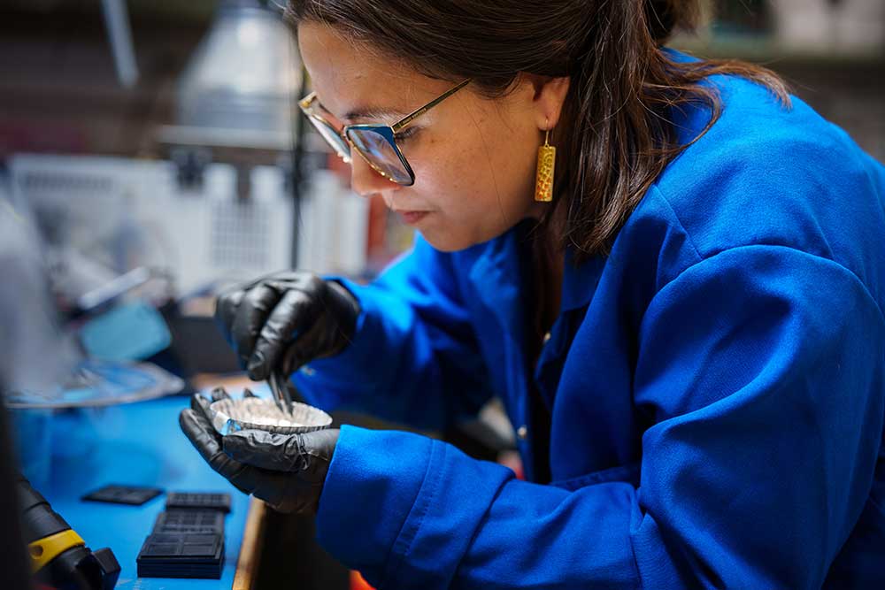
The sensing component consists of a porous, sponge-like material designed to chemically trap sarin and its chemical cousins.
This porous material, called a sol-gel, resembles spray insulation foam. The precursor chemicals are sprayed from a specialized nozzle onto a structure resembling two metal combs with interleaved teeth called an interdigitated electrode, said Philip Miller, a Sandia biomedical engineer on the project. The coated electrode is heated, causing the carrier liquid to evaporate and creating an open “popped bubble” structure.
“The porosity of the material creates more spots for the chemical of interest to land on,” Philip said. “The more molecules the sensor can measure, the faster the alert it can provide. If the sensor is worn on someone’s lapel, it can provide a ‘get out of Dodge’ alert. If the sensor is in the field, it can provide a warning to stay away.”
When a molecule of sarin binds to the sol-gel between the electrode’s teeth, the material’s electric properties change. This property, called capacitance, is detected by the rest of the sensor using minimal power, Philip said.
The team also explored using a different electrical measurement called impedance, which uses more power but is more selective. This would be valuable if the chemical of concern is similar to common airborne chemicals, Mieko said.
The development of the sol-gel material was funded by Sandia’s Laboratory Directed Research and Development program in an earlier project.
Converting chemical to electronic signals
The Sandia team collaborated with a professor and graduate student at the University of Virginia to design a readout integrated circuit that can detect changes in the sol-gel and convert them into useful signals while consuming minimal power, Mieko said.
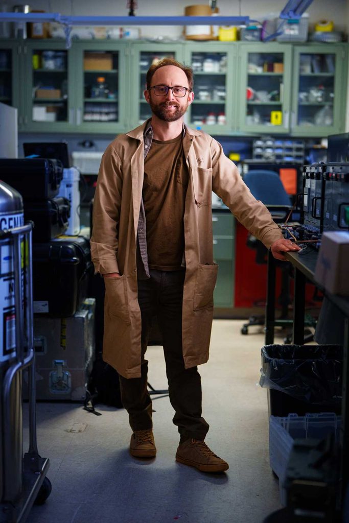
This was important because a readout integrated circuit typically consumes the most power in a sensor system, said Jesse Moody, a Sandia sensor engineer who led the circuit design.

“Essentially, we needed to develop a device that can detect very minute changes in that capacitive sensing film and convert that into useful digital information in an extremely low-power manner,” Jesse said. “That was the main electronics challenge of the project.”
The circuit was designed using structures on the scale of 65 nanometers, 1,500 times smaller than a human hair and three times smaller than the smallest transistor available from Sandia’s Microsystems Engineering, Science and Applications Complex’s fabrication facilities. This size was chosen to allow the sensor system to operate faster while using less power, Mieko said.
The circuit can quickly check the status of 10 chemical sensing channels in a few thousandths of a second, Jesse said. The development of the ultra-low-power readout integrated circuit built on prior LDRD and DOD projects in low-power sensing, he added.
The circuit design was fabricated at Taiwan Semiconductor Manufacturing Co., one of the world’s most advanced microchip fabrication facilities. Typically, it costs about $1 million to have a custom microchip fabricated at such a foundry; however, for this project, the Sandia team shared the initial cost with other companies as part of a multi-project wafer, Mieko said.
Usually, these multi-project wafers are diced, and each company receives only the square millimeter segments — about the size of a sharpened pencil tip — containing their design, Jesse said. However, these tiny pieces are challenging to handle and build on, even when inserted into a slightly larger package with connections called a silicon interposer, Mieko said.
For this project, the researchers had the other companies’ designs removed with a high-power laser and developed an innovative method to fill in the gaps with a polymer, allowing them to work with and build on a full silicon wafer, Mieko said.
Testing the full sensor
After resolving issues with the polymer planarization, the team assembled the sensor system. They compared the sensor system constructed via the heterogeneous integration pathway — from the tiny chips in a silicon interposer — with a monolithic sensor where everything was built on the same wafer.
The final monolithic sensor system measured 1 by 1 inch, while the heterogeneous test system was 10 times larger, Mieko said. She added that had the team optimized the heterogeneous sensor system, they could have reduced its size to about twice that of the monolithic sensor.
The monolithic sensor system used 30.9 nanowatts of power per sensing channel and had an area of 43 microns per channel. It ultimately consumed slightly more power per channel than the heterogeneous system due to a power leakage issue that the team didn’t have time to fully resolve, Mieko said. Once they optimize the monolithic system further, it should use less power than the heterogeneous system because direct connections require less power.
Since the proof-of-concept sensor system was successful, the team is exploring additional funding sources to continue developing ultra-low-power, long-lasting chemical sensors, Mieko said. The sensor system could be adapted with other chemically selective materials to detect multiple chemicals of concern in the same device, Philip said.
“The novelty of integrating the low-power microcontroller and the sol-gel sensor was a really cool project to work on,” Philip said. “Doing system-level sensor work is hard and doing it in this innovative way is especially challenging. I think we have a nice path forward to realize a functional device with additional support.”
The project was funded by Sandia’s LDRD program.