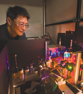
Jeff Tsao (1120) looks over a set-up used to test diode lasers as an aternative to LED lighting. (Photo by Randy Montoya)
Semiconductors are sneaky. Little by little they permeate your life, unnoticed until you stop and think. Remember mammoth cell phones and boxy computers? Remember being lost? “Our lives become more convenient, flexible, dynamic, and agile every day,” says Sandia Fellow and materials scientist Jerry Simmons (7000). “Semiconductors are the reason why.”
All modern electronics need semiconductors, which at the most elemental level simply switch electricity on and off. At opposite ends of the electrical spectrum are conducting materials, such as copper and aluminum, used in wires through which electricity is sent, and insulators that keep electricity from flowing out of the wires, causing shocks. “In between are semiconductors that can switch back and forth from conducting to insulating,” Jerry says. “When hooked together in complex ways, you get high performance computing. But semiconductors serve other functions like optical communications, imaging, and switching electrical power — also known as power electronics. As the semiconductors get more efficient, so do entire systems.”
Silicon, as in Silicon Valley, has long been the go-to semiconductor material for computing and power electronics. But a new generation of materials is taking hold that could lead to smaller, lighter, more powerful, and versatile devices. The rising stars are III-Vs, graphene, wide bandgaps, and metamaterials, each of which will push electronics, and modern life, to new places.
III-V: See the light
Jerry says one area in which silicon falls short is the handling of optical processes. “There are a lot of applications where you want something to absorb a particle of light or emit a particle of light,” he says. “People have used various non-silicon semiconductors to do that.”
Those innovations helped revolutionize telecommunications because optical fibers use light to carry computer signals. “The Internet is based on semiconductor devices that absorb a photon on the receiving end or emit a photon on the transmitting end,” Jerry says. “It was a generation of semiconductors worked on in the 1970s and ’80s that allowed optical internet communication to take place.”
Sandia is developing optical materials that will do even more. One innovation is solid state lighting powered by a new class of III-V semiconductors, so called because they combine elements from groups III and V of the periodic table. Using indium gallium nitride and aluminum gallium nitride, Sandia engineers have made some of the first high-intensity blue and ultraviolet light-emitting diodes, or LEDs.
“We had to learn how to grow the material thick enough to make an LED inside a growth chamber,” Jerry says. “You have different layers in the LED structure. The thickness of the quantum wells has to be well defined and controlled to within a single atomic layer.”
Sandia was a pioneer in that material system and helped make possible the white LEDs that are penetrating the market, replacing incandescent and fluorescent bulbs. Also developed were LEDs in ultraviolet wavelengths used in military applications and to purify water.
Researchers are extending the same gallium nitride-based materials into power electronics. “Instead of an information signal in your computer — tiny little currents of micro- or nano-amps — we’re looking at switching hundreds of amps to supply electricity from the grid to entire neighborhoods,” Jerry says. “The materials will make everything smaller, lighter, more efficient, and more reliable.”
Graphene: Strength in layers
Graphene is a one-atom-thick layer of the mineral graphite in which carbon atoms are arranged in a hexagonal pattern. It’s strong, light, and nearly transparent, an excellent conductor of heat and electricity with the potential to create ultra-small and fast components in electronics. Wafer-scale graphene can be engineered and integrated to other semiconductors, producing tailor-made components for applications in such areas as spintronics, biosensing, and bioanalytics.
“Graphene is just in its infancy, but the potential number of applications is mind-blowing. Because it is only one atom thick, it is easy to modify the surface or the edges of a strip of graphene and control its properties. So this can make very tiny, low-power switches,” Jerry says. “Or you can put two layers of graphene on top of each other and make a photon detector.”
Metamaterials: Second nature
Metamaterials are engineered to have properties not found in nature. Atoms and their arrangement in a material determine its properties. “It turns out you can make artificial atoms by shaping the material on a nanoscale, and as long as the shaping is significantly smaller than the wavelength of the energy it’s interacting with, it looks homogenous,” says Rick McCormick, senior manager in Radiation, Nano and Optical Sciences Dept. 1110. “You can’t tell the difference between the atomic response and the response of the shaping.”
By changing geometry at the nanoscale, materials can be artificially engineered to create a response that doesn’t exist in nature. “It opens the door to making artificial atoms at artificial frequencies,” Rick says. “Theoretically, that gives you a big knob to turn on material properties. We’re not stuck with what nature gave us.”
An example of such a property is the way a material responds to light. “Normally, when light passes through glass, like a prism, the light gets bent in a certain direction,” Rick says. “By using metamaterials, we can make the light bend in an opposite direction to what occurs in nature. This allows us to do new things with light including non-visible light, like infrared and radio waves, that were never imagined before.”
Examples include ultra-thin lenses, ultra-efficient cell phone antennas, and ways to keep satellites cool and photovoltaics more efficient. A recent Sandia Grand Challenge research project headed by Rick and funded through the Laboratory Directed Research and Development (LDRD) program advanced the state of the art in metamaterials from two-dimensional metafilms to three-dimensional materials, research that won an R&D 100 award.
The work led researchers to look at optics in new ways, including using metamaterials in an invisibility cloak to shield something from view by controlling electromagnetic radiation.
“Metamaterials have given us a bunch of new theoretical, computational, and experimental tools to explore the way light interacts with matter at a very small scale,” Rick says. “Now we can play with that in a new way.”
Wide bandgap: Hot topic
Electronic bandgap is a fundamental materials property. Wide-bandgap (WBG) materials such as silicon carbide and gallium nitride are semiconductors with bandgaps significantly greater than that of silicon. Wide bandgaps have already revolutionized lighting. But as transistors, or switches, in modern power electronics they also have the potential to vastly improve the performance of electrical power grids, electric vehicles, motors in buildings for elevators and HVAC systems, and even computer power supplies.
WBG materials can handle high temperatures and voltages, properties that could lead to simpler, less costly power conversion systems. WBG has the potential to substantially reduce the estimated 10 percent energy loss between generating electricity and transmitting it into a home or business. A wide bandgap allows faster switching.
“In a decade or two the giant transformers in your neighborhood distributing power from the electric grid to homes, that now weigh 10,000 pounds, will be replaced by things the size of a suitcase that weigh 100 pounds,” Jerry says.
And if electric vehicles could tap the potential for WBG power electronics to withstand higher temperatures, they might not need a liquid cooling system, reducing the system’s complexity and improving vehicle range because the car would weigh less.
Modern family
Jerry says Sandia is looking ahead to new classes of semiconductor materials that could help meet the Labs’ national security mission. Photon detectors are an example. “New photon detectors can image battlefields or landscapes in frequencies that we haven’t looked at before,” he says. “It’s a new generation of materials that gives us that capability.”
Where is the next generation of semiconductors leading? Jerry says to dramatic changes in the way people live. Some revolutions transform life in a striking way, as in buying an LED light bulb that uses less energy and saves money. Others sneak up, such as the realization over time that cell phones do much more in a much smaller package.
“Semiconductors have progressed over time to the point that the density of transistors and computing chips is mind-boggling,” Jerry says. “They are embedded in systems like cars and cell phones and home appliances. They allow us to have our modern-day lifestyle.
“But we always have to be out on the frontier looking for the newest discoveries and picking things to develop further. So if we talk about semiconductors again in two or three years, the topics will likely be dramatically different but equally exciting.”