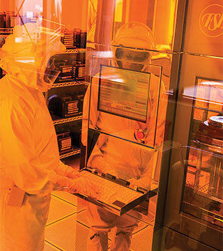
MESAFAB WORKER Penny Moore (1747) loads a cassette into a photolithography machine at the MESAFab, which is now producing base wafers for Application-Specific Integrated Circuits for the nuclear weapons program. Planning and preparation for production took years and involved more than 100 people. (Photo by Lloyd Wilson)
Sandia’s Microsystems and Engineering Sciences Applications complex has begun making silicon wafers for three nuclear weapon modernization programs, the largest production series in MESA’s history.
MESA’s silicon fab in October started producing base wafers for Application-Specific Integrated Circuits (ASICs) for the B61-12 Life Extension Program (LEP), W88 ALT (alteration) 370, and W87 Mk21 Fuze Replacement nuclear weapons. Planning and preparation took years and involved more than 100 people.
“We left no one untouched. If you were standing still, you got something to do,” says Jayne Bendure (1747), who was in charge of organizing 1,000 line items that had to be checked off before wafer production began.
Chief of Staff Dave Sandison (110), a senior manager at MESA’s Silicon Fab when the manufacturing readiness process began in July 2011, says detailed requirements for making war reserve-quality ASICs produced a gigantic list “in regular 12-point font about 4 feet long that went down the wall in my office.”
He implemented weekly meetings to review what had been accomplished and what was on tap for the coming week. The meetings focused on hitting deadlines and determining what was needed to stay on track, which convinced him and his successor, Mike Daily, that they needed more people. “You start to see the same people’s names show up every week, and they’re on a gazillion things,” Dave says.
“It was a multiyear program executed with precision and dedication,” says Gil Herrera, director of Microsystems Science &Technology Center 1700. “I’m very, very proud of the team. Now the hard part begins: We’ve got to make the parts.”
Center of Labs’ microsystems work
MESA is the center of Sandia’s investment in microsystems research, development, and prototyping. The 400,000-square foot complex of cleanrooms, labs, and offices houses the design, development, manufacture, integration, and qualification of trusted microsystems for national security applications.
MESA includes the Silicon Fab (SiFab), completed in 1988, and the Compound Semiconductor MicroFab, completed in 2006.
The SiFab, certified by DoD as a trusted foundry, develops and produces technologies for radiation-hardened complementary metal-oxide semiconductor (CMOS) integrated circuits and MEMS (micro-electro-mechanical systems). The MicroFab is a green-certified plant for III-V compound semiconductor material processing, post-silicon wafer processing, and advanced packaging, and for heterojunction bipolar transistor (HBT) production. Both fabs conduct R&D for future nuclear weapon and broader national security applications.
Kaila Raby (1754), manager for the Product Realization Team for ASICs, calls the production start a huge milestone. The SiFab will make ASICs through 2018 with the plant running its normal schedule of 24 hours a day, five days a week. In addition, the MicroFab is preparing to begin producing HBT integrated circuits in April, the first time MESA will produce HBT products for the stockpile, Kaila says.
Ten different silicon ASIC products go into the work on the B61-12, the W88 ALT, and the Mk 21 Fuze systems, Kaila says. Seven of the 10 ASICs have base wafers that are customized into product-specific designs during later production, she says. It’s these base wafers that the SiFab started manufacturing.
Sandia has invested in new manufacturing tools and processes for MESA, including 2-D marking, similar to bar-coding, for individual devices; an electronic production control system; automated lot acceptance support systems; streamlined quality management; and a greater focus on preventing defects, Gil says.
“A lot of things we’ve been working on for the last few years came together, and we’re doing all this while minimizing impacts to our other work for national security customers and the research mission,” he says.
Identifying production needs as multiyear project
MESA SiFab finished wafer fabrication for the W76-1 nuclear weapon in 2009, and began identifying manufacturing needs for the B61 and W88 programs, says manager Dale Hetherington (1746). Dale and manager Alan Mitchell (1747) credit success to the hard work of many people within the fab organizations including the equipment maintenance, process, and engineering staff.
“A large part of our mission is research and development and work for other customers besides the nuclear weapons program, so while we’ve been getting ready for this NW production and doing a 1,000 line-item production plan, we’ve still been manufacturing prototypes for the NW complex, for other missions around Sandia, and other labs as well,” Dale says. “So it’s not as if we shut down and did nothing but get ready for production.”
Volume for ASIC production will be more than three times that of the W76-1 production. MESA uses a build-ahead process: build many wafers and store them so they’re ready when needed.
“We typically build early because the wafers have to be diced into chips, the chips packaged and delivered to subsystem customers, and those subsystems then integrated into higher-level systems,” Dale says. “We have a production plan that factors in all the various chips for the B61, W88, and W87 programs.”
Production required prototyping in advance so designs were in place and ready to manufacture, and setting up quality systems and making sure they were rigorously documented, Alan says.
Wafer production is a critical part of the ASIC process but is only one step toward the final product and acceptance by NNSA. “While we build the wafers in our fab, when we’re done with them they have to be electrically tested, they need burn-in and reliability evaluation, they need packaging, so there are multiple sets of work activities from initial customer engagement through the design phases and into manufacturing,” Alan says.
MESA does it all: R&D, production, and development
Senior manager Paul Raglin (1210) points out MESA’s fabs are unique: They do R&D and production of ASICs and HBTs, all in-house with trusted components. “We can go directly into the stockpile with all the certifications,” he says.
MESA receives about $50 million a year through NNSA’s Readiness in Technical Base and Facilities (RTBF), Paul says. While RTBF provides base-level funding, the W88 and B61 programs furnish additional money for staff and materials.
The Sandia silicon fab revitalization (SSiFR) program has pledged $150 million over seven years to replace aging tools and transition MESA to 8-inch wafers by about 2020, Paul says.
A manufacturability review in late 2011 evaluated how various areas and tools operated. Curt Dundas (1746) says that snapshot became the basis for deciding what needed improvement and what could affect the SiFab’s ability to increase manufacturing capacity. The team worked down the list of needed improvements, evaluating any significant change to make sure it wouldn’t cause problems, he says.
“In manufacturing, it’s always about continuous improvement,” Curt says. “You’re never done. You just arrive at the point of a new snapshot.”
Jayne began organizing line items in August 2012 so the fab could switch from producing a primarily R&D line to an NW line. She says, however, most processes for controls, repeatability, and documentation already existed. “We reviewed everything, we improved the things we thought we needed to improve for NW, and we worked with our technology development group [1760] to make sure we were solid on what we needed to do.”
The plan required identifying tasks and who could keep those moving and involving enough people to get everything done on time. “It was a lot of work but having it structured like that was the only way to do it. People don’t mind hard work if they see you marching toward a big goal,” Jayne says.
She credits the production start to early planning, the structured plan, and senior management support. “But if not for the ability of the hands-on folks on the floor we would never have been successful in the time we had,” she says.