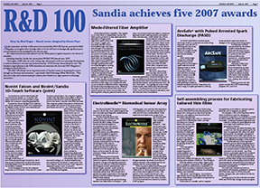
Sandia researchers and their collaborators have received five R&D 100 Awards, presented by R&D Magazine to recognize what its judges deem to be the 100 most technologically significant products introduced into the marketplace over the past year.
The valued awards have been referred to as the Nobel prizes of applied research or the Oscars of invention.
Including these five, Sandia has accumulated 80 R&D 100 Awards since 1976.
“Once again, DOE’s labs are at the cutting edge of innovation with new technology developments to enhance America’s economic and national security,” DOE Secretary Samuel Bodman said. “My heartiest congratulations to the DOE researchers and scientists who have won R&D Magazine’s prestigious awards this year.”
“The R&D 100 Awards are an important metric of Sandia’s success in impacting the nation through our discovery and innovation,” says Sandia Chief Technology Officer Rick Stulen. “They also serve a key role in demonstrating to industry that Sandia is an eager partner in technology maturation.”
Novint Falcon and Novint/Sandia 3D-Touch Software (joint)
Novint Falcon and Novint/Sandia 3D-Touch Software (joint), is a controller that makes interactive 3-D touch possible in high-fidelity for consumer computing applications.
Founded by former Sandian Tom Anderson, and jointly submitted for R&D 100 consideration by Nathan Golden (10104 ) and industrial partners, Novint’s software is largely based on technology originally developed at Sandia and exclusively licensed to Novint for commercialization.
Haptics is the science and art of providing touch sensations with computer-generated environments so that when virtual objects are touched, they seem real and tangible. While the current primary focus of the commercial technology is computer games, there are more serious uses in which the technique could make inroads. An example might be a medical training simulator in which a doctor can feel a scalpel cut through virtual skin, feel a needle push through virtual tissue, or feel a drill passing through virtual bone. All of these types of interactions would be felt almost indistinguishably from the real-life interactions the simulator emulates.
As the handgrip is moved, the computer keeps track of a 3-D cursor. When the 3-D cursor touches a virtual object, the computer registers contact with that object and updates currents to motors in the device to create an appropriate force to the device’s handle, which the user feels. The computer updates the position of the device, and updates the currents to the motors a thousand times a second (i.e., at a 1 kilohertz rate), providing a very realistic sense of touch. Three electrical motors are connected to the three arms extending out of the device, with one motor connected to each arm. The three arms are connected to the device’s handle. At any given cycle, or 1/1000th of a second, the device can create a force on the handle in any direction of any magnitude, up to the maximum force.
Haptics is applicable across nearly all areas of computing including video games, medical training, scientific visualization, CAD/CAM, computer animation, engineering design and analysis, architectural layout, virtual toys, remote vehicle and robot control, automotive design, art, medical rehabilitation, and interfaces for the blind, to name a few. The word ‘haptics’ derives from the Greek “haptikos,” meaning to grasp, touch, or perceive.
Funding sources for the work include LDRD and DOE Defense Programs.
Mode-Filtered Fiber Amplifier
Mode-Filtered Fiber Amplifier: The capability of coiled fibers to dramatically increase the useful power produced by fiber lasers has led to fabrication of high-power, high-beam-quality lasers that are compact, rugged, and extremely efficient. Prior to this breakthrough, fiber lasers were thought to be restricted by fundamental physical limitations of the fiber to low output powers and pulse energies. Specifically, the small, single-mode fiber core (typically less than 10 microns in diameter) was unable to generate or transmit high optical powers without being damaged or inciting parasitic nonlinear processes. Increasing the core size increased the laser power, but only at the expense of beam quality, a tradeoff that was prohibitive for most applications.
In 2000, Sandia and Naval Research Laboratory researchers demonstrated that bend loss from a coiled, large-core (multimode) fiber can act as a kind of distributed filter, suppressing all but the desired fundamental mode. Breaking the single-mode limit allowed fiber lasers to be scaled in power by a factor of more than 100, allowing these uniquely practical sources to displace conventional solid-state lasers in numerous applications and enabling entirely new applications. The discovery, which defied the conventional wisdom of the time, earned a patent in 2002 for Jeff Koplow and Dahv Kliner (both 8368), and Lew Goldberg, the inventors listed on the current R&D 100 Award. The technique has become the de facto worldwide standard for power scaling of fiber lasers. The first commercial license for the invention was granted in 2005, and the first commercial products were offered by coapplicants Nufern and Liekki in 2006. Three other companies have licensed and commercialized the invention.
The mode-filtered fiber laser has high electrical efficiency and optical gain, low waste-heat generation, broad wavelength coverage, and diffraction-limited beam quality (the theoretical limit) that is insensitive to vibrations, thermal fluctuations, and optical power level. All this, notes Dahv, “in a package an order of magnitude smaller than traditional solid-state laser sources.” Funding sources for the work include LDRD, DoD’s Air Force Research Laboratory, and the National Science Foundation.
ElectroNeedle™ Biomedical Sensor Array
The ElectroNeedle™ Biomedical Sensor Array is a device that, when pressed against the skin, can make rapid diagnostic measurements in a point-of-care setting.
The ElectroNeedle patch (Lab News, July 22, 2005 can detect and identify biological markers just beneath the skin’s surface. Because the electrochemical analysis is accomplished in situ, the need to withdraw body fluid is eliminated. The height of the needles, adjustable during microfabrication, allows the biological recognition layer to be placed in intimate contact with the appropriate tissue beneath the skin’s surface. For example, interstitial fluid in the epidermal layers of skin may be accessed for the measurement of small molecules such as glucose, while blood in the deeper dermal layers can be accessed for the measurement of larger molecules such as proteins.
By combining electrochemical measurement techniques with well-defined recognition chemistries and an easy-to-use sensor, a range of biologically important species can be detected. Potential biomarkers and bioagents include carbohydrates, electrolytes, lipids, enzymes, toxins, proteins, viruses, and bacteria in a patient’s blood or interstitial cellular fluid. This will provide a painless and rapid measurement of biologically relevant molecules without having to extract fluids for later analysis.
ElectroNeedle arrays are produced using standard microfabrication techniques — photolithography, etch, and thin-film deposition — permitting low-cost, batch production of these devices when commercialized. What makes the microfabrication unique is the microneedle material, a commercially available glass wafer — Foturan® — that can be photo-patterned and etched to make hollow microscopic needle structures that are then filled with metal to form the sensing electrodes. These microneedles are sharp enough to be inserted into the skin but rugged enough not to bend or break. Because the metal microneedle passes all the way through the glass substrate, electrical connections are made to the back of the substrate and do not interfere with the sensing needle tip.
With one patent granted and three pending, the application was submitted by Steve Casalnuovo (1714) for principal developers that include David Ingersoll (2546), Chris Apblett (1815), Stanley Kravitz (ret.), Jeb Flemming (former Sandian), Colin Buckley (former student intern), and Carrie Schmidt (1723).The work has been funded by Sandia’s LDRD program.
ArcSafe© with Pulsed Arrested Spark Discharge (PASD)
ArcSafe© with Pulsed Arrested Spark Discharge (PASD) is a patented electrical wiring diagnostic tool effective in detecting and then locating wiring insulation defects in complex wiring systems, including commercial and military aircraft.
PASD sends a high-voltage but extremely short-duration pulse along wires to encourage a spark breakdown at the slightest break in insulation. This causes a momentary short circuit and reflection of energy back to sensors to locate the defect, serving as a warning before a short might appear under normal operating conditions. Because the spark is so brief, it has about the same energy as a spark generated by walking across synthetic carpet and causes no damage to the wiring system being tested.
Development of PASD was sponsored by the Federal Aviation Administration (FAA) and has been incorporated into a portable diagnostic system by Astronics Advanced Electronics Systems Inc., a leading developer of aircraft electronics and diagnostics.
Says project lead Larry Schneider (1650), “PASD shows tremendous promise as the world’s only effective diagnostic capable of detecting and accurately locating such hard-to-find insulation defects as breached insulation, chafing, and insulation cracks.”
Funding sources for this project include the DOE Nuclear Energy program, FAA, and DoD.
Self-assembling process for fabricating tailored thin films
Self-Assembling Process for Fabricating Tailored Thin Films involved development of a simple soft coating process that forms optical, electrical, and magnetic thin films from self-assembled nanoparticles.
Led by Hongyou Fan (1815-1), with Bruce Burckel (1815), Jeff Brinker (1002), and Earl Stromberg of Lockheed Martin Aeronautics, the researchers developed a wet-solution-based process employing self-assembly to create engineered nanocomposite thin films with tunable properties by varying particle composition, sizes, shapes, and particle packing density and geometry.
“Our nanoparticle surface chemistry enables dispersal in readily available commercial solvents, allowing easy and rapid production of films through spin, dip, or spray coating under ambient conditions,” says Hongyou.
With the addition of secondary organic polymers or inorganic components, the nanoparticles self-assemble into ordered arrays embedded in a matrix of the secondary component that provides additional function and robustness in mechanical stability, and durability.
“The result,” says Hongyou, “is an ordered, high-density nanocomposite film where the constituent materials are controllably incorporated on the nanometer scale.”
Semiconductor, metallic, and/or magnetic nanoparticles can be added to optimize optical, electrical, and/or magnetic properties.
For example, a film can be deposited and its index of refraction tuned by changing its nanoparticle composition, concentration, or both to exactly match the required index of refraction of a surface, yielding an optimal single-layer anti-reflective coating on optical glasses as well as on high-index substrates, such as germanium windows.
Furthermore, the added flexibility and control over thin-film properties opens the door for engineered thin films with multiple functions. For example, nanoparticle optical films can be made hydrophobic to avoid fogging and icing problems that deteriorate optical performance of the devices.
“The broad reach of this rapid self-assembly process, delivering performance across multiple markets, at radically lower cost, in an environmentally friendly manner, warrants serious consideration as a top innovation in this decade,” says Walt Werner, a principal engineer for Lockheed Martin (Maritime Systems and Sensors).
This work leveraged the fundamental research of DOE’s Basic Energy Sciences program and LDRD aimed at developing multifunctional nanomaterials for microelectronics and optics as well as structure/property investigations of self-assembled nanomaterials.
The work is an extension of work on nanoparticle self-assembly published in Science in 2004 (Lab News, April 30, 2004) led by Jeff Brinker, Hongyou Fan, and students and faculty from UNM.
Funding sources for the work have included LDRD and DOE’s Basic Energy Sciences program.