Thin film work is poster child for getting R&D to industry
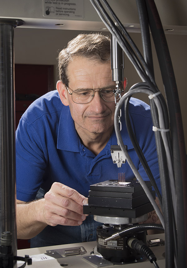
SANDIA RESEARCHER Paul Vianco works on thin films, nanometer-thick layers of metal that can be defined into precision electrical circuits. He won the Surface Mount Technology Association’s 2015 Best of Proceedings award and will be honored with other winners at the association’s meeting in September. (Photo by Randy Montoya)
Sandia researcher Paul Vianco sees his work on thin films as a poster child for the way research and development based on nuclear weapons work can boost US industry.
Since the 1970s, Laboratories researchers have taken studies originally performed to support the weapons program and published or presented parts of the work at technical conferences. Paul (1831) calls that passive tech transfer.
“Engineers would just fill rooms. They wanted to hear what we were doing, not only because our research represented the ‘latest-and-greatest,’ but more so because it was applied technology,” he says. “This was information that folks ate up because they could take it back to their companies and put it directly to use on their products.”
Paul recently won the Surface Mount Technology Association’s 2015 Best of Proceedings award for the paper “Establishing a Ti-Cu-Pt-Au Thin Film on Low Temperature Co-Fired Ceramic Technology for High-Temperature Electronics.” Co-authors were Jerome Rejent (1831), Alice Kilgo, Bonnie McKenzie, and Amy Allen (all 1819); Mark Grazier, recently retired from Sandia; and William Price of the Kansas City National Security Campus (KCNSC) and Esteban Guerrero, now retired from KCNSC. The winners of the Best Papers awards will be honored Sept. 27 at the association’s conference in Rosemont, Illinois. Paul also won the Best of Proceedings paper in 2012.
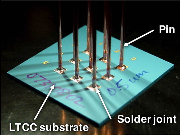
Thin films are nanometer-thick layers of metal that can be defined into precision electrical circuits similar to traditional printed circuit boards. Instead of a laminated or built-up copper conductor circuit, a thin film is patterned into a circuit through photolithography techniques. The benefit is miniaturization with finer lines and spaces, so the electronic component can be made smaller and do more at the same time.
“Smaller components weigh less and use less power,” says Paul. “We reduce what industry refers to as ‘SWaP,’ or size, weight, and power.”
Data could help further develop components
Sandia’s paper provides the electronics industry with data that can be used to further develop thin film-on-low temperature co-fired ceramic (LTCC) components – called hybrid microcircuits – for high-temperature electronics. Paul envisions a new generation of such LTCC components that will combine miniaturization, functionality, and the ability to withstand harsh environments, and which are fabricated by commonly used photolithography processes.
“The solder interconnection reliability data will enable use of these products in applications that include down-hole oil and gas exploration as well as renewable energy development,” Paul says. Such hybrid microcircuits also have significant potential for sensors and communications electronics in space probes, he says.
Sandia has been collaborating with the Kansas City National Security Campus since KCNSC’s breakthrough development of LTCC technology on thin film a few years ago. The research was funded by the nuclear weapons life extension program at Sandia as well as Sandia’s and KCNSC’s Enhanced Surveillance Campaigns, which support stockpile stewardship. KCNSC built the LTCC and deposited the thin films, while Sandia developed and implemented test procedures and used its advanced microanalysis capabilities for failure mode analyses.
Paul praised the collaboration.
“It’s really a case where we took the application, understood what information was needed to ensure producibility and reliability of the solder interconnections, and developed a test in collaboration with our KCNSC partners. The result was strength and failure analysis information that significantly enhanced the ability of Sandia to design new components and of KCNSC to fabricate them into high-reliability products,” he says. “We’ve sort of come full circle: We identified the need, developed an experiment, and obtained test data that supported the application. Publishing the results made the data available to the US electronics industry.”
Offers industry new applied technology
The award-winning study evaluated the mechanical properties of solder joints made to a thin film conductor pattern deposited on the surface of an LTCC substrate. Co-fired means individual layers, stacked on one another, are fired together at high temperatures to create the internal, multilayer circuitry and interconnections that are hallmark LTCC technology. Paul and his colleagues developed a standard method to assess solder joint strength on the advanced thin film circuits. The approach provides a way to define assembly processes and determine the long-term reliability of solder interconnections for critical, high-frequency components.
“Thin film conductors are not a new circuit technology, but they are still in relative infancy in the high-reliability electronics industry,” he says. “A lot of hybrid microcircuits still rely upon the old thick film conductor technology, which uses screen or stencil printing to define the electrical circuit. We’ve used it for years on high-frequency components. But it’s limited in terms of achieving better SWaP for those products because we can’t miniaturize it very much more than we’ve already done.”
The electronics industry wants to improve product performance, but often hasn’t fully appreciated the intricacies of interconnections-plus-thin films as a materials system, he says. “It’s been kind of a mystery in terms of how solder joints made to thin film conductors stay attached to the LTCC substrate, but I think they now see that what we’re doing is valuable in furthering this technology. For those who never thought of using thin film-on-LTCC, those folks are saying, ‘Maybe now we do know enough about this technology to try it on our products.’”