Precise atom implants in silicon provide first step toward quantum computers
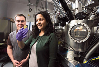
Post-doc fellows Meenakshi Singh and Jose Pacheco stand in front of Sandia’s ion beam generator. Project PI Meenakshi holds a sample qubit structure embedded in silicon. (Photo by Randy Montoya)
Sandia researchers have supported post-doctoral fellow Meenakshi Singh in taking the first step toward creating a practical quantum computer, able to handle huge numbers of computations instantaneously. Here’s the recipe:
A “donor” atom propelled by an ion beam is inserted very precisely into industry-standard silicon.
The donor atom, in this case antimony (Sb), carries one more electron (five) than a silicon atom (four). Because electrons pair up, the odd Sb electron remains free.
Instruments monitor the free electron to determine if, under pressure from an electromagnetic field, it faces up or down, a property called “spin.” Electrons in this role, called qubits, signal “yes” or “no” from the subatomic scale and are the information bearers of a quantum computer.
The ability to precisely place a donor atom in silicon means that it should be possible to precisely place another donor atom just far enough away, in the “Goldilocks” zone where communication is neither lost through distance nor muffled by too-close contact. Attempts to do this will be made later this year, says Meenakshi. Qubits “talking” to each other are the basis of quantum computing circuits.
Quantum dot operates like a transistor
The successful Sandia first step, reported in mid-February (vol. 108, issue 6) in the journal Applied Physics Letters, makes use of electromagnetic forces provided by a neighboring quantum dot pre-embedded in the silicon. The quantum dot — itself a tiny sea of electrons — contains a variety of energy levels and operates like a transistor to block or pass the qubit.
If an available dot energy level is compatible with the electron, the transistor gate is effectually open and the electron jumps into the dot. If not, the electron stays put. That action is reported back to the surface by a photodiode sensor sensitive to current flows rather than photon movement. Because of the multiple “gates” in the quantum dot, many electrons at different energy levels could pass through the transistor, or be denied passage, theoretically making possible an extremely wide array of information processing
“Our method is promising because since our method reads the electron’s spin rather than its electrical charge, its information is not swallowed by background static and instead remains coherent for a relatively long time,” Meenakshi says. “Also, we use silicon as our basic material, for which commercial fabrication technologies are already developed, rather than employing superconducting components, which can be expensive.”
Precisely place donor atoms
A third unique quality of the Sandia work is its ability to precisely place donor atoms exactly where they should be, rather than relying on a buckshot approach that places qubits where they only statistically average to Goldilocks distances.
While components of this experiment have been demonstrated before, this is first time that all the components have worked together on a single chip, with researchers knowing accurately the vertical and horizontal placement of each qubit, instead of mere statistical approximations.
Sandia researcher and paper author Mike Lilly expects that “the Sandia technique will allow fabrication of more complicated multi-qubit structures and do so at higher yield than existing donor-implant approaches.”
Components of the successful device were fabricated in Sandia’s MESA facility. The donor atoms were placed in Sandia’s Ion Beam Laboratory, under the supervision of post-doc Jose Pacheco. Experiment measurements were made at the Sandia/Los Alamos Center for Integrated Nanotechnologies, a user facility supported by DOE’s Office of Basic Energy Sciences.
The method in its entirety is straightforward but requires a range of technical expertise and machinery, Meenakshi says. “We used ion beams, silicon fabrication facilities, low-temperature measurements, and simulations. It’s hard to find a non-commercial place outside of a national lab that can do all of this.”
The work was supported by NNSA, DOE’s Office of Science, and the Center for Integrated Nanotechnologies.