![[navigation panel]](http://www.sandia.gov/images/label.gif)
|
|
|
|
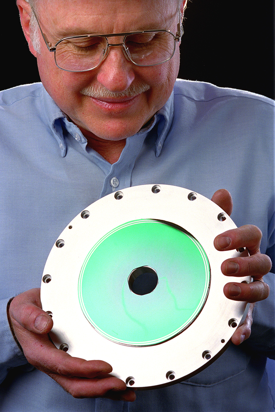
Cool tool to improve microchip production patented by Sandia ALBUQUERQUE, N.M. -- A device expected to be potentially less expensive and more effective than any on the market in helping cool silicon wafers during the chip manufacturing process has been patented in prototype by researchers at Sandia National Laboratories. The device is called an electrostatic chuck because it electrostatically clamps onto a silicon wafer, allowing the temperature to be regulated with confined helium gas, says Bob Anderson, who holds the patent with Carl Seager. Because the Sandia chuck face is made of the same materials as computer chips -- silicon, silicon dioxide and silicon nitride -- and is fabricated with well-understood silicon chip technology, manufacturing costs should be far lower and batch contaminations far fewer than those for a conventional chuck's sprayed-on overcoat of diverse materials currently used by industry. The Sandia chuck should be able to operate at higher temperatures more suitable to modern wafer processing. It also clamps and releases wafers more quickly than other methods, decreasing processing time. Prototype Sandia chuck faces that demonstrated this rapid operation were fabricated at Sandia's Microelectronics Development Laboratory. Sandia is a laboratory of the Department of Energy (DOE), which with SEMATECH funded this research. SEMATECH is a non-profit consortium of 11 semiconductor manufacturers, based in Austin, Texas.
Like sticking a balloon to a sweater
"An electrostatic chuck and the wafer held on it are essentially a big capacitor," said Sandia project leader Alan Hurd of the method in general. "The force generated within the capacitor tends to squish it together." The Sandia system holds several advantages over conventional designs -- also electrostatic -- of Japanese manufacture.
Tiny silicon islands
The chuck face of the in-use design consists of a composite material, randomly sprayed on a base plate and then polished. It too supports the wafer at just a few bumps, but these are necessarily a bit conductive. "Put another way," says Anderson, "the coating on the in-use chuck needs some electrical conductivity so that high fields can be developed between the chuck face and the wafer intended to be held, but an excessive conductivity would short out the power supply that generates the clamping field." Therefore the conductivity must be kept fairly small, to limit leakage, and results in appreciable time delays for applying or releasing the clamping force. When the voltage is turned off, the wafer on a conventional chuck might remain for a time, "stuck like a balloon to a wall," says Anderson. "Our design circumvents that problem, by micromachining the chuck face to create non-conductive raised areas -- the islands -- while the bulk of the chuck facing remains electrically conductive." According to Anderson, "The composite material on a conventional chuck is complicated, difficult to make, and raises the possibility of contamination by foreign material." The useful temperature range of this composite is also quite restricted. The Sandia design, instead, uses a chuck face that is tolerant of high temperatures. In fact, it may be possible to develop a chuck that will operate up to 600 degrees Celsius. In addition, "You can't rejuvenate the conventional base plate when it wears down over time -- it's got to be thrown away," says Hurd. The well-understood fabrication process for creating the Sandia chuck face should significantly reduce the cost of chuck replacement. Sandia is a multiprogram DOE laboratory, operated by a subsidiary of Lockheed Martin Corp. With main facilities in Albuquerque, N.M., and Livermore, Calif., Sandia has major research and development responsibilities in national security, energy, and environmental technologies and economic competitiveness. Media contact: Neal Singer, nsinger@sandia.gov, (505) 845-7078 Technical contacts: Bob Anderson, raander@sandia.gov, (505) 844-7676 Carl Seager, chseage@sandia.gov, (505) 844-9168 |
|
Back to top of page |
![[electrostatic chuck]](images/chuck.gif)