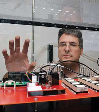
Caption: BOB KAPLAR (1768) peers at a test circuit built under a Grand Challenge Laboratory Directed Research and Development project to evaluate the switching performance of wide bandgap and ultra-wide bandgap power semiconductor devices. (Photo by Randy Montoya)
Sandia researchers are working on wide bandgap materials that someday could replace silicon as the backbone of the power semiconductor industry.
Wide bandgap (WBG) materials such as silicon carbide (SiC) and gallium nitride (GaN) could potentially vastly improve the performance of the electric power grid, solar photovoltaics, and electrical motors, and help meet the aviation and automotive industries’ need to use less energy. GaN has already enabled a revolution in efficient lighting technology and serves as the heart of widely available bright light-emitting diodes. These semiconductor materials have bandgaps significantly wider than that of silicon, the material on which most power systems and modern computers are based.
Bandgap is a fundamental materials property. WBG and ultra-wide bandgap (UWBG) materials are attractive as transistors, or switches, because they can handle higher temperatures and voltages with less degradation.
UWBG materials have potential applications in nuclear weapons and defense systems as well as in future energy systems because of their potentially high radiation resistance and the prospect of enabling smaller and lighter power systems. However, the materials still require a lot of research, says Sandia Fellow Jerry Simmons (1000).
Sandia is researching SiC and GaN, but it’s also working to leapfrog over these next-generation materials to the generation-after-next, UWBG materials such as aluminum nitride (AlN).
AlN and GaN are compatible enough to be mixed. That allows researchers to take small steps toward developing AlN by gradually increasing the amount of AlN versus GaN to study behavior and the effect of lattice mismatch between the semiconductor and the material it’s grown on, says Bob Kaplar (1768), principal investigator for a Grand Challenge Laboratory Directed Research and Development (LDRD) project on UWBG materials.
Wide bandgap materials have performance advantages
Estimates predict SiC could perform 100 times better than silicon for power switching, GaN could be 1,000 times better than silicon, and AlN could be 10,000 times better than silicon. However, their potential can’t be tapped until researchers better understand how the materials work, develop mature techniques to process them, and address reliability concerns, particularly for high-consequence uses.
Sandia researchers have conducted wide bandgap research for nearly two decades. Early work largely focused on solid-state lighting and ultraviolet light emitters, then research expanded into such areas as photodetectors and radio frequency transmitters.
The UWBG grand challenge is the flagship project for Sandia’s Power on Demand Research Challenge aimed at developing electrical power systems with the smallest size and weight, while handling the largest possible amount of energy. The research challenge tackles underlying fundamental science questions, engineering applications, and technical challenges for devices, materials growth, and power systems.
The grand challenge is a major investment and an opportunity to create a team with a single vision, says Manager Rick Schneider (1120), program lead for the grand challenge and part of the research challenge team. Technology from the grand challenge could advance the research challenge’s effort in power electronics. Power on Demand’s other two focus areas are advanced battery research and photovoltaic research.
The grand challenge covers three areas: materials growth; device design, fabrication, and testing; and defects and radiation resistance. It explores ways to grow UWBG materials with fewer defects and different device designs to exploit the properties of materials other than silicon.
Among others leading teams or research focus areas, Andy Allerman (1126) works on growth of wide and ultra-wide bandgap materials; Andy Armstrong (1123) measures densities and energy levels of defects in these materials; Art Fischer (1123) and Albert Baca (1766) research device architectures and fabrication; and Jason Neely (1353) evaluates device performance.
“DOE already supports the wide bandgap manufacturing industry, so there’s a national priority around this technology,” Rick says. Sandia is unique in the DOE complex for its semiconductor capability — the Microsystems and Engineering Sciences Applications (MESA) complex; the Center for Innovative Nanotechnology it operates with Los Alamos National Laboratory; and Sandia’s long history of innovative semiconductor devices and materials. “We come in with a lot of relevant experience and a rich base for power electronics,” Rick says.
The largest support for the Wide Bandgap Grand Challenge within Sandia comes from nuclear weapons programs, and Defense Systems & Assessments is interested as well, he says. Nationally, the research has potential impact on the grid, transportation technology, and energy efficiency.
Once Sandia establishes a core ultra-wide bandgap capability, “We have the potential to create very unique radiation-hardened components. It may be a very good opportunity to think about a trusted manufacturing enterprise within Sandia in partnership with MESA. That’s a 5- to 10-year vision for Sandia with the potential for external collaboration and industry outreach,” Rick says.
Performance issues include defects, integration into larger systems
Although some devices using SiC and GaN are on the market, thorny problems remain, Bob says. Common performance issues include defects, incompatibility with the microelectronics substrates on which the materials are grown, and the impact of integrating a device into a larger system. Sandia researchers can evaluate those problems impartially, building on knowledge and capabilities gained in decades of nuclear weapons work.
Improvements in WBG or UWBG materials could cascade into improvements in an entire system.
For example, WBG materials could potentially reduce the estimated 10 percent energy loss that occurs between generating electricity and transmitting it to a home or business. A wide bandgap allows faster switching, which could reduce the size of bulky passive elements, Bob says. Thus, WBG devices could mean higher reliability, smaller size, and less expensive systems.
Likewise, if electric vehicles could tap the potential for WBG and UWBG power electronics to withstand higher temperatures, they might not need liquid cooling systems, resulting in smaller and lighter electronic systems. That could reduce the system’s complexity and improve vehicle range because the car would weigh less.
But materials compatibility also can be a problem in part of the transistor called the gate, which turns the switch on and off. A critical part of that is the gate oxide, or insulating material. Researchers are exploring various substances as possible gate oxides.
For silicon and SiC, the gate oxide is silicon dioxide. While it’s a match for silicon, silicon dioxide is a more complex interface for SiC because the presence of carbon results in more material defects that can affect the transistor’s electrical behavior, Bob says. Oxide physics on GaN pose an extremely complicated materials science problem that will require atomic-level understanding before such devices will be practical, he says.
Researchers studying how to grow wide bandgap materials better
There also is no widely available, low-cost, large-area GaN substrate, the crystal on which semiconductor material is grown. That lack affects the type of transistor structure that can be made. Bob led an LDRD project to explore how to design, grow, and fabricate GaN devices on GaN substrates.
Silicon and SiC are grown on very pure single-crystal silicon or SiC wafers purchased commercially, meaning the starting material and grown layers are basically the same. However, without low-cost, large-area GaN wafers, GaN traditionally is grown on slices of sapphire, silicon, or SiC. Since the atomic spacing between the wafer and GaN isn’t the same, GaN ends up with tiny defects, Jerry says. Defects limit the type of transistor structure that can be made.
That’s why device performance doesn’t live up to predictions, Jerry says. Defects also impair reliability, a critical issue for uses such as the electric grid and transportation.
Until researchers can figure out how to grow large-area bulk GaN substrates inexpensively, they use such tricks as etching minuscule fingers into the substrate so GaN grows on top of the fingers and merges, reducing the strain inside, Jerry says.
WBG and UWBG devices must be integrated into larger systems. A switch, for example, fits with other parts into a system that includes high-voltage switches and low-voltage sections such as microprocessors, with a buffer or driver in between. Everything in a highly integrated system must withstand high temperatures. While WBG materials are robust at such temperatures, the packaging or semiconductor chip casing is not as resilient, Bob says. Sandia is studying robust packaging approaches.
“With expertise spanning fundamental materials growth all the way through systems integration, Sandia is uniquely qualified to tackle the entire range of challenges in this emerging field and is well-positioned to be the leading laboratory in an area of increasing national importance,” Bob says.