Suppose you believe — as many researchers do — that nanowires will be the electrical current-carriers of the future for certain types of solar arrays, batteries, telephones, and tiny portable computers. But perhaps you also suspect — as many researchers do — that strange and unpredictable effects may take place in the currents carried by these nanowires when placed in proximity to each other — the sine qua non for carrying out their business.
So you’d want to measure the possible changes in voltage of one wire as caused by another, to determine how significant the current boost or drag, so you can allow for it in designing your device. But you have a problem. The best test method available involves putting a charged piece of material called a gate between two nanowires on a single shelf. The gate, flooded with electrons, acts as a barrier: It maintains the integrity, in effect, of the wires on either side of it by repelling any electrons attempting to escape across it. But the smallest wire separation allowed by the gate is 80 nanometers. A much smaller gap is necessary for verisimilitude with expected future devices.
Simple but brilliant test design
Now consider instead this simple but brilliant test design: What lead researcher Mike Lilly (1132) and co-workers at McGill University envisioned was to put the nanowires one above the other, rather than side by side, by separating them with a few atomic layers of very purely grown crystal. The result? Nanowires separated vertically by only 15 nanometers. And because each wire sits on its own independent platform, each can be independently fed and controlled by electrical inputs varied by the researchers.
The researchers found, as reported online at DOI: 10.1038/NNANO.2011.182, and in the upcoming December 2011 Nature Nanotechnology, highly significant effects: Positive voltage boosts could be as high as 25 percent on the second wire.
The work required the crystal-growing expertise of John Reno (1132), the fabrication and measurement skills of McGill doctoral student Dominique Laroche, and elements of previous work by Jerry Simmons (1120).
“There are all sorts of people working on nanowires,” says Mike. “They’ve been doing it for 20 years. At first, you study such wires individually or all together, but eventually you want a systematic way of studying the integration of nanowires into nanocircuitry. That’s what’s happening now. It’s important to know how one-dimensional (1-D) wires interact with each other rather than regular wires.
A 1-D wire is not the common thick-waisted household (3-D) wire, which allows current to move across, vertically, and forward, nor is it your smaller flattened micron-sized wires (2-D) in typical electronic devices that allow electrons to move forward and across but not up and down. In 1-D wires, the electrons can only move in one direction: forward, like prisoners coming to lunch, one behind the other.
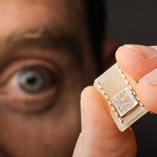
Though the gallium-arsenide structures used by Mike are fragile, nanowires in general have very practical characteristics — they may crack less than their bigger cousins, they’re cheaper to produce, and offer better electronic control. But it’s as a problem in basic science that their characteristics fascinate Lilly.
The Coulomb drag effect
“In the long run, our test device will allow us to probe how 1-D conductors are different from 2-D and 3-D conductors,” says Mike. “They are expected to be very different, but there are relatively few experimental techniques that have been used to study the 1-D ground state.”
One reason for the difference is the Coulomb force, responsible for what is termed the Coulomb drag effect regardless whether the force hastens or retards currents. Operating between wires, the force is inversely proportional to the square of the distance; that is, in ordinary microelectronics, the force is practically unnoticeable, but at nanodistances, the force is large enough that electrons in one wire can “feel” the individual electrons moving in another placed nearby.
The drag means that the first wire needs more energy because the Coulomb force creates, in effect, increased resistance. “The amount is very small,” says Mike, “and we can’t measure it. What we can measure is the voltage of the other wire.”
There are no straightforward answers as to why the Coulomb force creates negative or positive drag, but it does.
What’s known, Mike says, is that “enough electrons get knocked along that they provide positive source at one wire end, negative at the other. A voltage then builds up in the opposite direction to keep electrons in place.”
The so-called Fermi sea — a 3-D concept used to predict the average energy of electrons in metal — should totally break down in 1-D wires, which instead should form a Luttinger liquid, says Mike. A Luttinger liquid is a theoretical model describing the interactions of electrons in a 1-D conductor. To better understand the Luttinger liquid is Mike’s underlying reason for the experiment.
Having an interest on many levels proved useful because making the test device “took us a very long time,” says Mike. “It’s not impossible to do in other labs, but Sandia has crystal-growing capabilities, a microfabrication facility, and support for fundamental research from DOE’s office of Basic Energy Sciences (BES). Their core program is interested in new science and new discoveries, like the work we’re doing in trying to understand the fundamental ideas behind what is going on when you’re working with very small systems.”
Device fabrication was conducted under a user project at the Center for Integrated Nanotechnologies, a DOE Office of Science national user facility jointly run by Sandia and Los Alamos national laboratories. The device design and measurement were completed under the DOE Office of Science BES/Division of Materials Science and Engineering research program.