Solar ‘glitter’ supported by microelectronics and MEMS techniques
The idea of building a solar collector out of pieces the size of glitter at first seems peculiar. How would the tiny pieces be joined together? How would electricity be harvested from each piece? The costs seem prohibitive to wire the back of each tiny cell so that electrons — converted from incoming photons — can be properly channeled.
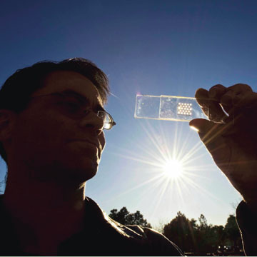
Project lead Greg Nielson holds a solar cell test prototype with a microscale lens array fastened above it that together will help create a concentrated photovoltaic unit . (Photo by Randy Montoya)
Yet Sandia benchtop aggregations of exactly such tiny photovoltaic (PV) collectors have resulted in inexpensive and efficient electricity-generating cells that have aroused commercial interest.
The cells are fabricated of crystalline silicon, using microelectronic and microelectromechanical systems (MEMS) techniques.
Project lead investigator Greg Nielson (1749-2) says the research team has identified more than 20 benefits of scale for its microphotovoltaic cells. These include new applications, improved performance, potential for reduced costs, and higher efficiencies.
For large-scale power generation, says project participant Murat Okandan (1749-2), “One of the biggest scale benefits is a significant reduction in manufacturing and installation costs compared with current PV techniques.”
Part of the potential cost reduction comes about because microcells require relatively little material to form well-controlled and highly efficient devices.
From 14 to 20 micrometers thick (a human hair is approximately 70 micrometers thick), they are 10 times thinner than conventional 6-inch-by-6-inch, brick-sized cells, yet perform at about the same efficiency.
“So they use 100 times less silicon to generate the same amount of electricity,” says Murat. “Since they are much smaller and have less mechanical deformations for a given environment than the conventional cells, they may also be more reliable over the long term.”
Another manufacturing convenience is that the cells, because they are only hundreds of micrometers in diameter, can be fabricated from commercial wafers of any size, including today’s 300-millimeter (12-inch) diameter wafers and future 450-millimeter (18-inch) wafers. Further, if one cell proves defective in manufacture, the rest still can be harvested, while if a brick-sized unit goes bad, the entire wafer may be unusable. Also, brick-sized units fabricated larger than the conventional 6-inch-by-6-inch cross section to take advantage of larger wafer size would require thicker power lines to harvest the increased power, creating more cost and possibly shading the wafer. That problem does not exist with the small-cell approach and its individualized wiring.
Other unique features are available because the cells are so small. “The shade tolerance of our units to overhead obstructions is better than conventional PV panels,” says Greg, “because portions of our units not in shade will keep sending out electricity where a partially shaded conventional panel may turn off entirely.”
Because flexible substrates can be easily fabricated, high-efficiency PV for ubiquitous solar power becomes more feasible, says Murat.
“Eventually units could be mass-produced and wrapped around unusual shapes for building-integrated solar, tents, and maybe even clothing,” he says. This would make it possible for hunters, hikers, or military personnel in the field to recharge batteries for phones, cameras, and other electronic devices as they walk or rest.
Storage at the chip level
Even better, such microengineered panels could have circuits imprinted that would help perform other functions customarily left to large-scale construction with the attendant need for field construction design and permits.
Says Sandia field engineer Vipin Gupta (6338), “Photovoltaic modules made from these micro-sized cells for the rooftops of homes and warehouse could have intelligent controls, inverters, and even storage built in at the chip level. Such an integrated module could greatly simplify the cumbersome design, bid, permit, and grid integration process that our solar technical assistance teams see in the field all the time.”
A commercial move to microscale PV cells would be a dramatic change from conventional silicon PV modules composed of arrays of 6-inch-by-6-inch wafers. However, by bringing in techniques normally used in MEMS, electronics, and the light-emitting diode (LED) industries, the change to small cells should be relatively straightforward, Vipin says.
Each cell is formed on silicon wafers, etched, and then released inexpensively in hexagonal shapes, with electrical contacts prefabricated on each piece, by borrowing techniques from integrated circuits and MEMS.
Offering a run for their money to conventional large wafers of crystalline silicon, electricity presently can be harvested from the Sandia-created cells with 14.9 percent efficiency. Off-the-shelf commercial modules range from 13 to 20 percent efficient.
A widely used commercial tool called a pick-and-place machine — the current standard for the mass assembly of electronics — can place up to 130,000 pieces of glitter per hour at electrical contact points preestablished on the substrate; the placement takes place at cooler temperatures. The cost is approximately one-tenth of a cent per piece with the number of cells per module determined by the level of optical concentration and the size of the die, likely to be in the 10,000 to 50,000 cell per square meter range. An alternate technology, still at the lab-bench stage, involves self-assembly of the parts at even lower costs.
Solar concentrators — low-cost, prefabricated, optically efficient microlens arrays — can be placed directly over each glitter-sized cell to increase the number of photons arriving to be converted via the photovoltaic effect into electrons. The small cell size means that cheaper and more efficient short focal length microlens arrays can be fabricated for this purpose.
Reduced costs
High-voltage output is possible directly from the modules because of the large number of cells in the array. This reduces costs associated with wiring, due to reduced resistive losses at higher voltages.
The project combines expertise from Sandia’s Microsystems Center, Photovoltaics and Grid Integration Department; the Materials, Devices, and Energy Technologies Group; and the National Renewable Energy Lab’s Concentrating Photovoltaics Group.
Involved in the process, in addition to Greg, Murat, and Vipin, are Jose Luis Cruz-Campa (1749-1), Paul Resnick (1749-1), Tammy Pluym (1746), Peggy Clews (1746), Carlos Sanchez (1746), Bill Sweatt (1512), Tony Lentine (1727), Anton Filatov (1749-1), Mike Sinclair (1816), Mark Overberg (1742), Jeff Nelson (6338), Jennifer Granata (6335), Craig Carmignani (6335), Rick Kemp (1815), Connie Stewart (1815), Jonathan Wierer (1123), George Wang (1126), Jerry Simmons (1120), Jason Strauch (1717), Judith Lavin (6338), and Mark Wanlass (NREL).
The work is supported by DOE’s Solar Energy Technology Program and Sandia’s LDRD program, and has been presented at four technical conferences this year.
The ability of light to produce electrons, and thus electricity, has been known for more than a hundred years.
Are there other applications beyond terrestrial solar power? “Absolutely!” says Greg. “We envision this technology impacting many areas of Sandia’s business including satellites and remote sensing, in addition to supporting warfighters.”