Improvements in the transistor of the future may not rely on decreasing its size but rather on a radical change in operation made possible by a quantum mechanical transistor created at Sandia.
The quantum mechanical transistor is the equivalent of turning on a light bulb without closing a switch: Electrons “tunnel” from path to path through a barrier that, according to classical physics, is impenetrable. The effect occurs with extreme rapidity.
Not science fiction any more
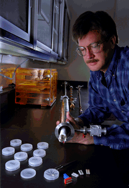
QUANTUM MECHANIC – Jerry Simmons inspects the end of a cryogenic sample holder for performing electrical measurements on the DELTT quantum mechanical transistor. Once loaded with DELTTs (from circular cases in foreground), the holder is lowered into a cryostat, allowing transistor performances to be tested at different temperatures.
(Photo by Randy Montoya)
The term “tunneling” may bring to mind moles or the highway department, but physicists use it to describe an effect in which particles, like electrons, appear in places where by rights they should not be able to go. In effect, they have tunneled under an energy barrier the same way cars use a tunnel to appear at a new location without having to drive over an impossibly high summit.
The atomic-scale effect is explained only by quantum mechanical principles.
“We have demonstrated real circuits that work and are easily fabricated,” says Jerry Simmons, leader of the Sandia development team. “It is not ready to be sold yet, but it is a significant advance.”
Reality, not just theory
The device, dubbed DELTT (Double Electron Layer Tunneling Transistor), offers promise of significant improvements in the speed of computers and in the accuracy of sensors.
Sandia has applied for one patent and is preparing others on the device. A paper on the DELTT has been accepted for publication by Applied Physics Letters. The work is funded by Sandia’s Laboratory-Directed Research and Development program, which funds speculative, defense-related research, and by Defense Programs Research Foundations.
According to Paul Berger, professor of electrical and computer engineering at the University of Delaware, “I was impressed by the multitude of possible uses of the DELTT device, as well as by its simplicity of connectivity.” Berger chaired the session at the International Electron Devices Meeting in Washington, D.C., late last year at which the first paper on the device was delivered.
A trillion operations a second?
The very fast device may run at a trillion operations a second, as have other, more primitive tunneling devices. This is roughly ten times the speed of the fastest transistor circuits currently in use. Actual speed has not yet been measured, says Simmons, because it is “not easy to measure such high speeds, which are near the limits of what can be measured with conventional equipment.” The device also runs at extremely low power – tens of millivolts and microamps – as compared with the few volts and milliamps needed by transistors currently in use.
That electrons can travel so rapidly in the DELTT gallium arsenide transistor means that normal electrical processes that slow down transmission of information – like scattering of electrons by crystal imperfections that behave much like potholes in the electrons’ pathway – can be minimized.
From Sandia’s point of view as a DOE national defense laboratory, the device might someday be put to work in satellites and smart missiles to process information faster, with less payload and much lower power consumption than today’s devices. The structure also could be modified for use as an optical detector in the far infrared. Incoming photons would be used to add energy needed for a transition between electron states, causing the device to turn on in only a narrow energy band.
Because the device is also tunable, it could act like an energy spectrometer on a chip. This could allow sensitive detection of chemical and biological species like nerve gas and anthrax, helping to combat bio- or chem-terrorists by allowing more rapid and reliable detection of minute concentrations of toxic materials at customs and airports, on the battlefield, and via airborne platforms.
Actual use of the transistor by industry may be years in the future because of other engineering problems to be tackled. These include questions of temperature – the device now works only at temperatures at or below 77 degrees Kelvin, though rapid improvement indicates it should be operating at room temperature by next year, says Simmons.
Another problem involves designing millions of such circuits on a chip, as is currently done with ordinary transistors. Because of the Sandia device’s multifunctionality – it has three positions, off-on-off, instead of the normal transistors’ two on-or-off states – the same amount of work can be performed with significantly fewer transistors, and chips would have to be completely redesigned.
The technique relies in part on the dual wave-particle nature of matter. In the device, two gallium arsenide layers, each only 150 angstroms thick, are separated by a 125 angstrom aluminum-gallium-arsenide barrier – the equivalent of the yards of two houses separated by a sturdy fence. Ordinarily, gallium arsenide electrons in one yard do not have the energy to climb the fence to reach the other yard. But the tiny thickness of the barrier causes the electrons to behave like waves, which can poke into the barrier.
When an electron is adjusted to have the same energy and momentum states in both regions – something that can be done by applying a voltage to these regions – it can pass from one region to the other without any scattering, as occurs in normal electron motion due to crystal imperfections. In effect, they tunnel under the barrier fence.
Previous tunneling transistor attempts had been made by researchers creating at least some layers side by side on a surface – too difficult a task for current technology to accurately manufacture repeatedly at 1,000 angstroms or the even smaller dimensions necessary. A novel design change allowed Sandia researchers to stack all DELTT layers vertically, using molecular beam epitaxy (MBE) or chemical vapor deposition (CVD), which enable single-atom layers to be grown. MBE and CVD are the same processes used to make, among other products, semiconductor lasers for compact disc players, and are readily available technologies.
Other members of the Sandia team include Mark Blount, Jeong-Sun Moon, Wes Baca (all 1112), Marc Sherwin (now at AMP-M/A-COM), Ken Lyo and John Reno (both 1113), and Joel Wendt and Mike Hafich (both 1314).