
Example files on this page
full input deck — Salinas_rtest/training/exampleproblem/material/piezoelectric/transient.inp
Single patch bimorph model — Salinas_rtest/training/exampleproblem/material/piezoelectric/single_patch.exo
11. Coupled Electro-mechanical Physics#
The term “piezoelectricity” refers to the production of electrical charges on a surface by the imposition of mechanical stress. Sierra/SD supports coupled electro-mechanical physics to simulate the electro-mechanical behavior of piezoelectric materials when subjected to an electric field or mechanical stress. One common application of piezoelectrics is in experimental modal testing. Due to the electro-mechanical stiffness coupling, piezoelectrics provide a convenient means to conduct structural dynamics tests since structural vibrations can be converted to electric potentials (i.e. voltages) which can then be stored and processed.
This section demonstrates how to use Sierra/SD to simulate exciting and measuring structural vibrations using voltages and piezoelectrics. A mechanical wave is generated from a prescribed voltage time-history using one piezoelectric tile. It passes through the aluminum barrier and excites the second piezoelectric tile. The deforming piezoelectric tile induces a time-varying electric charge at its surface that we output in terms of voltage.
The demonstration model is shown in Figure 11.1. Symmetry faces mark the surfaces with symmetry boundary conditions. The voltage input and response surfaces are indicated. The full input deck is also included.
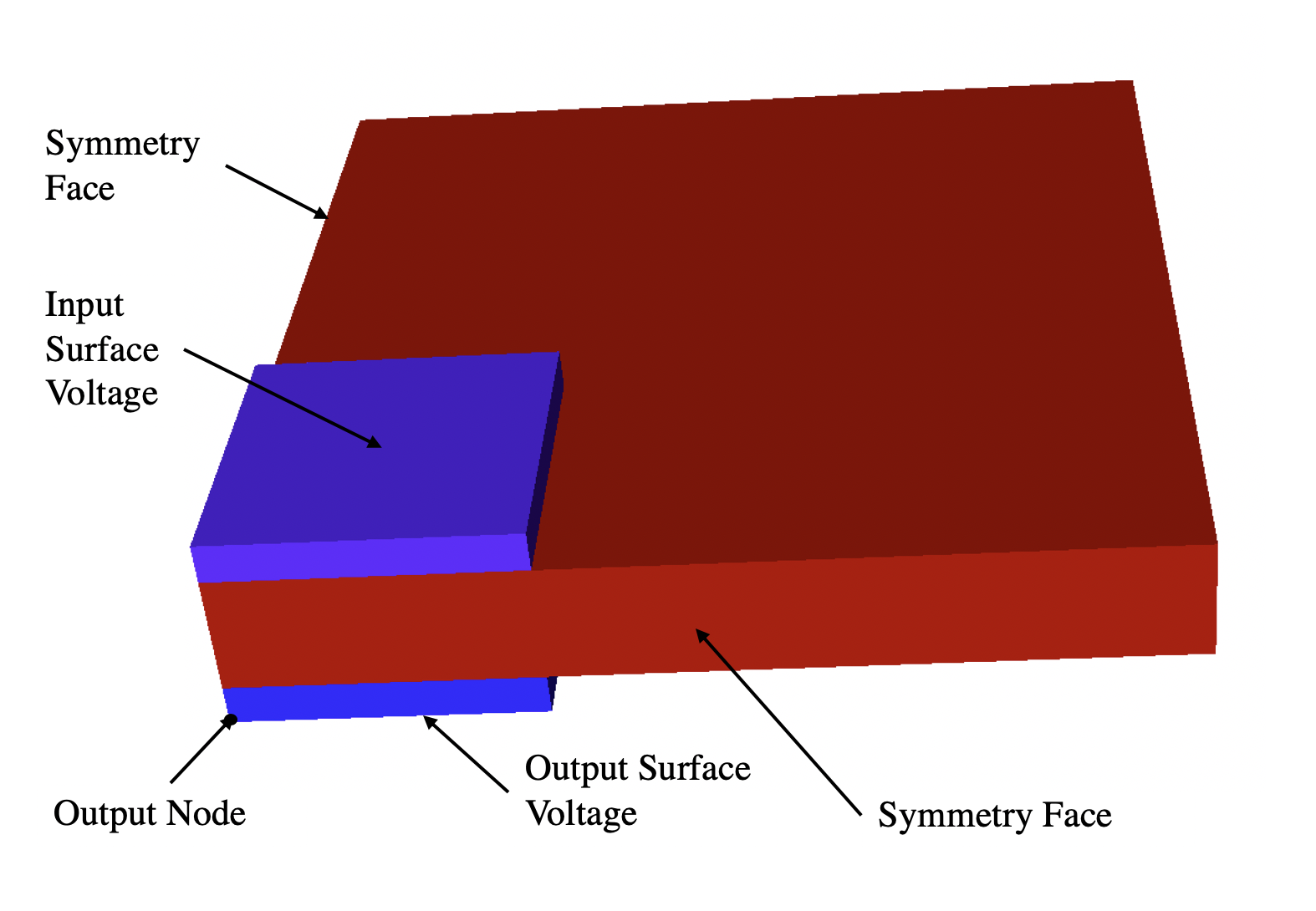
Figure 11.1 Single patch bimorph model#
11.1. Piezoelectric Material Input#
The piezoelectric material constitutive properties must include the orthotropic elasticity tensor (Cij), the permittivity tensor (permittivity_ij), and the piezoelectric coupling tensor (e_ij). Here is the material block for this input deck:
// {scale = 1e9}      // voltage unit scale

// {ep = 8.85418782e-12} // permittivity of free space
// {D11 = ep * 762.5 * scale * scale }
// {D33 = ep * 663.2 * scale * scale}

// {E11 = -5.20279 * scale}
// {E33 = 15.0804 * scale}
// {E15 = 12.7179 * scale}

MATERIAL PIEZOELECTRIC
  ORTHOTROPIC_PIEZOELECTRIC
    Cij = 1.39e11   .78e11  .74e11
                   1.39e11  .74e11
                           1.15e11
                            .25e11
                            .25e11
                            .31e11

    permittivity_ij {D11} 0    0
                    0    {D11} 0
                    0    0   {D33}

     e_ij =  0      0     {E11}
             0      0     {E11}
             0      0     {E33}
             0      {E15} 0
             {E15}  0     0
             0      0     0
    density = 7500
END
There are a few important details to note.
Careful consideration for the coordinate system should be taken when specifying the coupling matrix. The material’s poling direction is dependent on the coupling matrix, which should be specified with respect to the global coordinate system (unless a local coordinate system for that material block is specified). In this example, the piezoelectric material is poled in the global z-axis.
Since the permittivity matrix has units, its entries should be scaled by the permittivity of free space. In this example, we define a variable \(ep\) for the permittivity of free space.
We recommend changing the voltage units (volts \(V\)) to nanovolts (\(nV\)) where \(1\, nV = 10^{-9}\; V\). This scaling will significantly improve the condition of the system’s stiffness matrix and hence the convergence of the FE solver. See Section 11.4 for more details on solver issues related to piezoelectrics.
11.2. Boundary Conditions#
The voltage signal used to excite the mechanical wave is a Gaussian pulse defined by the superposition of a 10 kHz and 43 kHz sinusoidal waves weighted by a Gaussian pulse function (Figure 11.2). The Gaussian pulse is applied to the surface labeled Input Surface Voltage. In this example, we define the voltage time history explicitly with a function. Grounded voltage conditions are prescribed on the barrier surfaces. The following presents the boundary input including the symmetry boundary conditions.
BOUNDARY
  sideset 5 //symmetry boundary condition
    x = 0
  sideset 4 // symmetry boundary condition
    y = 0
  sideset 6    // voltage input
    transV = 1
    function voltage_input
  sideset 7  // grounded voltage
    V = 0
END

FUNCTION voltage_input
  type linear
  #include create_input_deck/voltage_input.inp
END
In addition to prescribing voltage boundary conditions, we also apply a voltage rigid set to enforce an equipotential surface at the voltage output surface. The surface of the piezoelectric device where voltage is measured is often plated with a purely conductive material such as copper; this physically enforces an equipotential surface. The voltage rigid set simplifies our model by enforcing the equipotential surface without having to model a super thin conductive layer. The rigid set is specified in this problem as follows:
RIGIDSET set1
  voltage
  sideset 8
END
11.3. Transient Response Results#
Figure 11.3 presents the voltage response at an arbitrary node located on the output surface. Since we used a rigid set, the voltage is equal at every node along that surface.
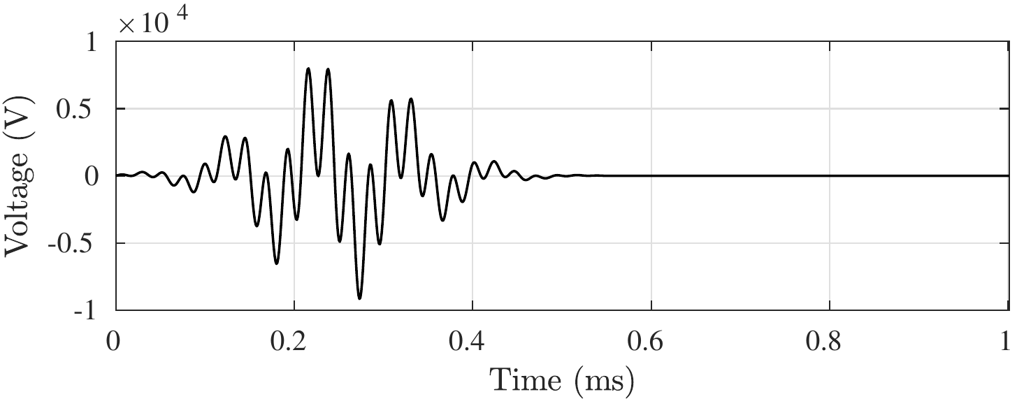
Figure 11.2 Time history of voltage input (Gaussian pulse).#
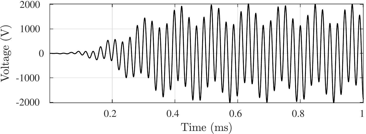
Figure 11.3 Time history of voltage response.#
11.4. Linear System Solver Issues and Recommendations#
Elastic and permittivity material properties can differ by tens of orders of magnitude, causing ill-conditioning of The coupled piezoelectric global stiffness matrix. To improve the matrix condition, we recommend scaling the voltage units (volts \(V\)) to nanovolts (\(nV\)). To scale voltage to nanovolts, the piezoelectric coupling matrix \(e_{ij}\) should be multiplied by \(10^{9}\) and the permittivity matrix by \(10^{18}\).
Another option to account for ill-conditioning is to use the gdsw solver with diagonal scaling. These solver parameters can be specified in the input deck as shown below. Diagonal scaling should be thought of as a band-aid. If the conditioning of the system can be fixed by scaling the underlying unit system, that is preferable to using diagonal scaling. The solver_tol option controls the tolerance to which the underlying linear system is solved. The default tolerance is \(1e-6\), a tolerance of \(1e-12\) will give a more accurate solution at the cost of increased computation time. One way to check the convergence of the solver is to see if changing the solver tolerance (\(1e-6 \rightarrow 1e-7\)) significantly changes the solution. If it does, a tighter solver tolerance is needed. We recommend contacting the Sierra/SD team (sierra-help@sandia.gov) in choosing an appropriate set of solver parameters.
SOLUTION
  directfrf      // solution method selected
  solver = gdsw  // solver specified
END

GDSW
  diag_scaling = diagonal // diagonal scaling turned on
  solver_tol = 1e-10      // convergence tolerance
END